Yagi-Uda Antennas · Volume 3
Feedpoint Impedance, Matching, and the Topology Families
Why parasitic loading collapses the driven element's Z well below 73 Ω, the mutual-impedance mechanism behind it, the gamma/hairpin/T-match/LFA matching menu done properly (the hairpin's shunt-inductor mechanism corrected), the LFA patent and market-share claims fact-checked, and the single-band/OWA/LFA/quagi topology families with their honest bandwidth tradeoffs
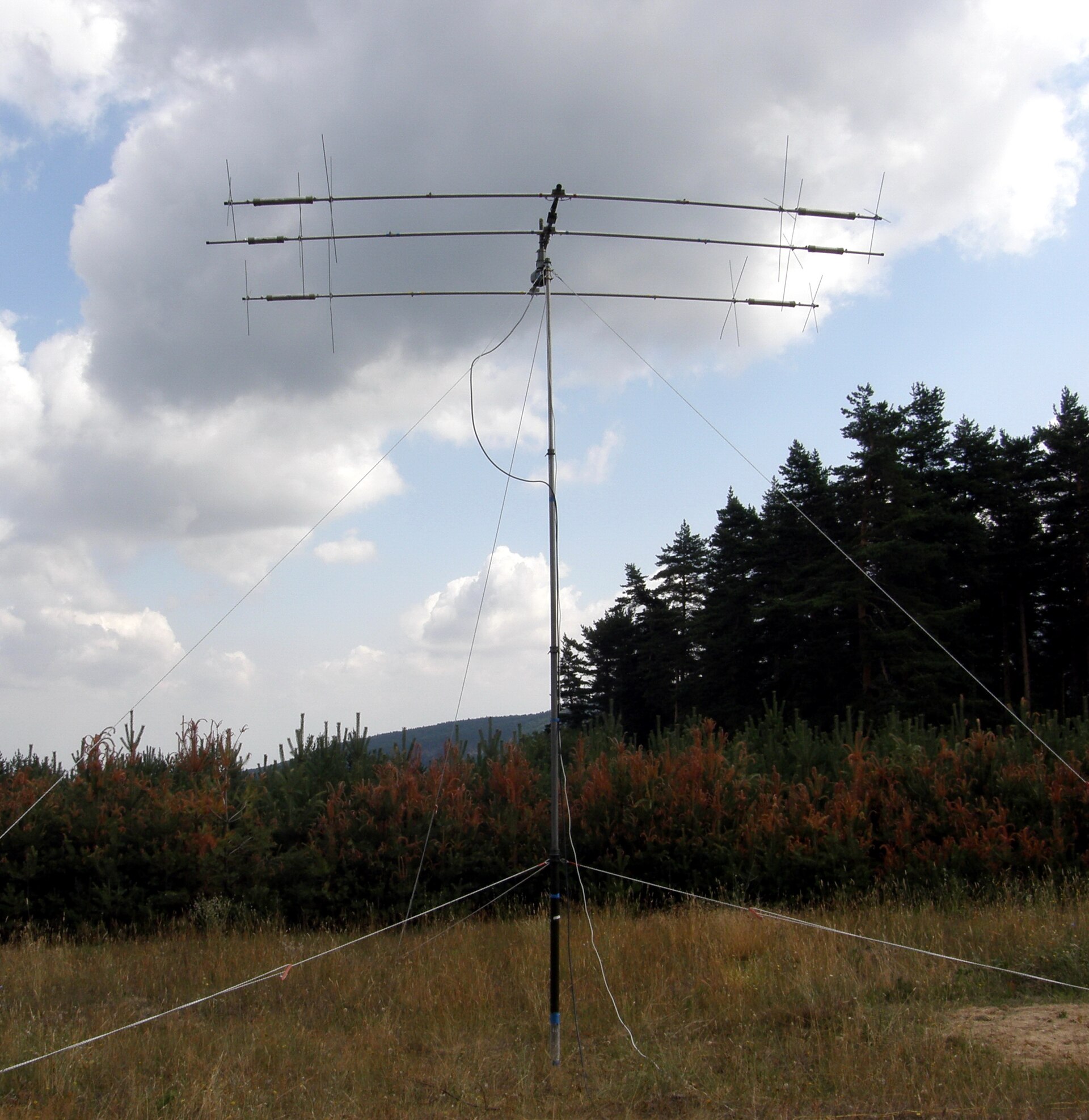
3.1 About this volume
Vol 1 established why a Yagi works at all — a driven element surrounded by parasitic reflectors and directors, each re-radiating a phase-shifted copy of the field it intercepts, summing to forward gain and a rear null. Vol 2 took that same array and asked what it radiates: gain, pattern, front-to-back, and the gain-versus-bandwidth tension that governs how tightly a designer can pack elements onto a boom before the pattern stops being usable. This volume asks a narrower, more mechanical question: what impedance shows up at the one point where you actually connect a feedline, and what do you do about it?
That question turns out to be more consequential than it looks, for a reason the parasitic-array picture makes almost obvious once you say it out loud: the very same tight electromagnetic coupling that produces a Yagi’s gain also reaches back into the driven element’s own terminals and changes what they look like electrically. A free-standing half-wave dipole feeds at a clean ≈ 73 Ω (the single-band dipole dive’s subject). Drop that same element into a Yagi, surrounded by a reflector and one or more directors close enough to do useful work, and the feedpoint resistance falls — often by a factor of two to five — before you’ve touched a matching network at all. Understanding why that fall happens, how far it goes, and what it costs the installer is this volume’s first job. The matching hardware that gets a 50 Ω coax feedline talking to whatever the array actually presents — gamma, hairpin, T-match, the loop-fed LFA driven element, and the folded-dipole step-up borrowed wholesale from the dipole world — is the second job, and it gets the same treatment the single-band dipole feedpoint volume gave the choke balun: worked mechanism, not just a name and a picture. The third job is to sort the resulting design space into families — single-band traditional, OWA, LFA, and the quagi/loop-Yagi — and to be honest about what each one trades away, including a hard look at one attribution claim (the LFA’s patent and its market position) that does not survive a fact-check unmodified.
Scope discipline matters here because this dive is being written across several volumes at once. The parasitic-array gain mechanism and the mutual-impedance framework this volume leans on belong to Vol 1; this volume does not re-derive them, only uses the result. The array’s gain, pattern, front-to-back ratio, and the gain-vs-bandwidth design tension at the level of “how many elements, how tightly spaced” belong to Vol 2; this volume’s own bandwidth section stays narrowly focused on what the feedpoint impedance and the matching network do to the SWR curve, not on re-litigating why long booms narrow patterns. What follows here is the feed: the number, the mechanism behind the number, and the five ways to get a coax happy with it.
3.2 The impedance-collapse mechanism — mutual coupling drives R down
Start from the coupled-circuit picture that Vol 1 sets up for the array as a whole and specialize it to the one terminal you can touch. Treat the driven element and each parasitic element as ports of a linear network, related by a mutual-impedance matrix: V_i = Σ_j Z_ij I_j. A parasitic element carries no external source, so its terminal voltage is zero — V_k = 0 for every reflector or director k — which is just the statement that a passive element is a plain conductor with nothing connected across its gap. That single constraint, applied to each parasitic element in turn and solved for its induced current in terms of the driven element’s current, and then substituted back into the driven element’s own voltage equation, produces the standard result for the impedance a source actually sees looking into the driven terminals:
Z_in = Z_11 − Σ_k (Z_1k · Z_k1) / Z_kk,
summed over every parasitic element k (the exact expression is more involved once inter-parasitic coupling is included, but the sign and the qualitative behavior survive that complication intact). Z_11 is the driven element’s own self-impedance — close to the free-space dipole’s 73 Ω for an isolated half-wave conductor of the same length and diameter. Every term in the sum is subtracted, and every term is positive for the geometries a Yagi actually uses (closely spaced, near-resonant-length parallel conductors), because that is exactly the coupling condition that produces constructive forward interference in the first place. Add a reflector: one term comes out of Z_11. Add a director: another term comes out. Add a second and third director, each one now coupled not only to the driven element but weakly to its neighbors too, and the correction grows further. The forward gain Vol 1 derives and the feedpoint-resistance collapse this volume derives are the same physical coupling, read off two different terminals of the same matrix. You cannot have the constructive re-radiation that produces gain without the identical mutual-impedance terms pulling the driven element’s own terminal resistance down — they are not two independent design axes to be traded against each other so much as two readouts of one underlying coupling strength.
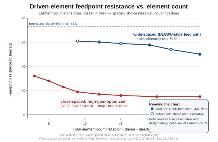
The magnitude of the correction terms is set by how tightly coupled the near elements are — chiefly the reflector-to-driven and driven-to-first-director spacing, since those two couplings dominate the sum (elements further out couple more weakly and contribute progressively smaller terms, the same diminishing-returns pattern Vol 2 documents for gain-per-director). This is the reason a single, clean “feedpoint resistance as a function of element count” table is the wrong way to think about the number, and it is worth being explicit that the widely-repeated shorthand figures for 5-, 9-, and 15-element Yagis are, at best, representative of one design philosophy rather than a physical law. The clearest illustration of the point is the contrast between the two dominant amateur long-boom traditions. K1FO-style designs (the Steve Powlishen tradition of closely-spaced, side-lobe-optimized long Yagis) deliberately use a tight feed cell and land the driven-element resistance down around 15–17 Ω even on quite long booms, matched up to 50 Ω coax through a step-up T-match or balun built for exactly that ratio. DL6WU-style designs (Günter Hoch’s wide-spaced tradition, the basis for most published wideband long-boom EME Yagis) use deliberately looser spacing through the same feed cell specifically to avoid that collapse — modeled feedpoints on 432 MHz DL6WU-derived arrays run 49.65 + j13.75 Ω at 10 elements, 57.93 + j10.14 Ω at 19 elements, and 51.42 + j3.80 Ω at 28 elements (read from Cebik/W4RNL’s published DL6WU-series table, whose models step in threes from 10 to 40 elements), holding close to a directly-feedable 50 Ω all the way out to boom lengths where a close-spaced design would have long since dropped into the teens. A more modest, commonly-quoted range for a modest 5- to 9-element close-coupled design — the territory a typical amateur commercial Yagi occupies — runs roughly 20 to 35 Ω, which is a defensible order of magnitude but should be read as “typical for this design family,” not as a number derivable from element count alone.
The practical consequence follows directly from the same physics and is worth stating plainly, because it is the reason this volume exists as a companion to Vol 2 rather than a footnote to it: a longer, higher-gain, tightly-coupled Yagi is harder to match, and the matching network’s own loss eats a growing fraction of the gain the extra boom length paid for. Treat the matching problem as a simple L-network transforming a low resistance R_s up to the 50 Ω line, and the network’s loaded Q is approximately Q = √(R_L/R_s − 1). At R_s = 35 Ω (a modest 5-element design), Q ≈ 0.65; at R_s = 25 Ω, Q ≈ 1.0; at R_s = 15 Ω (a tightly-coupled long-boom design), Q ≈ 1.53 — better than double the modest design’s loaded Q for the same 50 Ω target. A matching network’s fractional power loss scales with the ratio of its loaded Q to the real hardware’s unloaded Q (the gamma capacitor’s ESR, the hairpin conductor’s skin-effect resistance, the transformer core’s loss tangent) — component unloaded Q is a fixed property of real parts, so a network forced to run at twice the loaded Q dissipates a correspondingly larger share of the power reaching it as heat rather than radiation. None of this is a large effect on any single well-built Yagi — a properly silver-plated gamma capacitor or a fat hairpin conductor keeps the loss to a few tenths of a dB even at the tighter end — but it is a real, monotonic tax that grows with boom length exactly where Vol 2’s diminishing-returns curve says the marginal gain from one more director is already shrinking. The two effects compound: the last few directors on a very long boom buy less gain and lose more of it to the matching network than the first few did.
3.3 Direct feed and the folded-dipole step-up
The simplest matching network is none at all. Some designs — a deliberately wide-spaced DL6WU-family Yagi, an OWA design whose whole point is a flat, near-50 Ω impedance across the band (§8), or a short 2- or 3-element design where the parasitic loading has not yet pulled R far from 50 Ω — land close enough to the coax’s native impedance that a plain, unmatched connection is the right engineering answer. As with the single-band dipole and the quarter-wave monopole, “direct feed” still means a 1:1 current choke belongs at the feedpoint — the driven element is a balanced two-terminal load, coax is unbalanced, and nothing about parasitic loading changes that balance problem. Direct feed is the mechanically simplest option by a wide margin (no capacitor, no hairpin stub, no loop) but it constrains the designer: the driven-element length and the spacing to the nearest parasitic elements have to be chosen to land near 50 Ω, which is one more constraint competing against peak gain, F/B, and bandwidth in the same optimization Vol 2 describes.
When the driven element’s own resistance is well below 50 Ω but its reactance is small (a resonant or near-resonant length, not the deliberately-shortened case §5 develops), a folded dipole is the classic step-up. The mechanism is the single-band dipole variants volume’s subject in full — splitting the driven current between two closely-coupled parallel conductors shorted at both ends steps the feedpoint impedance up by (nominally) 4×, from ≈ 73 Ω to ≈ 290 Ω for an isolated half-wave folded dipole — and this volume does not re-derive it. What is worth stating here is how that step-up ratio interacts with a parasitically-loaded environment, because the two effects genuinely compound rather than one simply overriding the other: the 4:1 ratio (or a different ratio, achievable by using unequal-diameter conductors in the fold) applies to whatever self-impedance the loaded driven element would otherwise present, not only to the free-space 73 Ω figure. A driven element that would present, say, 18 Ω as a plain rod inside a tightly-coupled long Yagi presents roughly 4 × 18 ≈ 72 Ω once folded — a useful step most of the way back toward 50 Ω without any external network, gamma rod, or hairpin stub at all. This is exactly why several long-boom designs (and a number of commercial VHF/UHF Yagis) use a folded driven element specifically as a built-in impedance-recovery trick for parasitic loading, rather than for the “step up a 73 Ω dipole” reason the technique is usually taught. The tradeoff is mechanical: a folded element is two conductors, a shorting bar or plate at each end, and — because a folded dipole is inherently a balanced structure feeding a still-unbalanced coax — the same 1:1 current choke requirement, now paired with whatever step-up ratio the fold provides rather than a 1:1 ratio.
3.4 The gamma match
The gamma match solves the low-Z, shortened-driven-element problem with an asymmetric shunt-feed geometry, and it earns its long service history (standard on HF Yagis from the 1960s through the 1990s — Cushcraft, Wilson, Hy-Gain all built their beam lines around it) by being genuinely flexible: it can match nearly any driven-element impedance the parasitic array can produce, with only field adjustment and no redesign of the element itself.
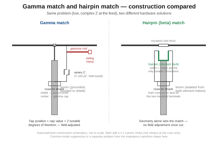
The construction is a short rod (the “gamma rod”) mounted parallel to and a few inches offset from one half of the driven element, bonded to that element’s tip and to the boom (which is itself bonded to the coax shield, at the driven element’s electrical center), with a sliding clamp partway along the rod’s length providing a tunable tap point, and a series capacitor (typically in the range of a few picofarads up to about a hundred, chosen for the frequency and power level) between the near end of the gamma rod and the coax center conductor. The tap position sets how much of the driven element’s current the gamma rod samples — moving the tap toward the tip sees a lower impedance, moving it toward the center sees a higher one — and the series capacitor cancels the inductive reactance the offset tap introduces, landing the combination on 50 Ω resistive. Two independent adjustments (tap position and capacitance) are exactly what is needed to hit an arbitrary complex target impedance, which is the source of the gamma match’s flexibility and also of its most common complaint: it needs field tuning, iteratively, with an antenna analyzer, and it is not a “cut it and forget it” part.
The weather and reliability failure modes are worth naming because they are the reason the gamma match has been steadily displaced at VHF and UHF by the hairpin and the LFA loop. The series capacitor is the weak point: a variable air or trimmer capacitor exposed to weather is a moisture-ingress and corrosion risk, and a fixed high-power capacitor sized for the legal amateur limit is itself an added cost and a component that can fail under RF voltage stress if undersized (§12 of the migrated seed material for this dive flagged 1–2 kW as a typical gamma-capacitor power ceiling, well below what the elements themselves handle). The sliding clamp is a second maintenance point — a mechanical connection exposed to the weather that can loosen, corrode, or shift under wind and ice loading, silently detuning the match without any visible sign until an SWR check reveals it. There is also a well-documented minor pattern asymmetry: because the gamma rod sits on only one side of the driven element, the structure is not left-right symmetric, and the near-field perturbation it introduces produces a small, measurable skew in the azimuth pattern relative to a symmetric matching scheme — rarely large enough to matter for a modest amateur Yagi, but a real, physical consequence of the asymmetric geometry rather than a myth.
3.5 The hairpin (beta) match — a shunt inductor against a deliberately capacitive load
The hairpin match is frequently described in the amateur literature as simply “an inductor that cancels the reactance of a shortened driven element,” which is true as far as it goes but skips the part that makes the mechanism worth understanding rather than memorizing: the same shunt inductance that cancels the reactance is also what steps the resistance up toward 50 Ω — they are not two separate actions, they are one action read two ways.
Start from the driven element deliberately cut a little shorter than the resonant length that would zero its reactance. A shortened element presents a capacitive reactance in series with its (already parasitically-lowered) resistance: Z_d = R − jX_c, with R well below 50 Ω and X_c positive. Converting to admittance, Y_d = 1/Z_d = G + jB, with both G and B positive — the capacitive load shows up as a positive (capacitive) susceptance in the admittance domain exactly as it does in the impedance domain. Now bridge a shorted stub — a plain U-shaped piece of wire or tubing, the “hairpin” — directly across the two feed terminals, in parallel with the driven element’s own impedance. A shorted stub shorter than a quarter-wavelength is a pure shunt inductor, contributing a negative (inductive) susceptance −jB_L to the parallel combination. As the hairpin’s dimensions (and therefore B_L) are tuned, the total admittance becomes Y_total = G + j(B − B_L).
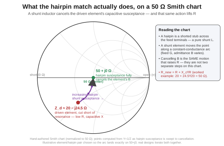
Here is the point that gets missed: because G is fixed by the driven element’s own R and X_c and does not change as the hairpin is tuned, sweeping B_L traces a path of constant conductance in the admittance plane — which, mapped back into the impedance plane the way a Smith chart always maps admittance to impedance, is a smooth arc, not a straight line, and that arc’s resistance rises monotonically as the susceptance is cancelled. At full cancellation (B_L = B, Y_total = G purely real), the resulting resistance is R_new = 1/G = R + X_c²/R — strictly larger than the starting R, by an amount set entirely by how much capacitive reactance the element was carrying. A concrete, illustrative worked example makes the arithmetic land exactly on 50 Ω: a driven element presenting Z_d ≈ 20 − j24.5 Ω has R/(R² + X_c²) = 20/1000 = 0.02 S, so full cancellation of its susceptance lands the total impedance at 1/0.02 = 50 + j0 Ω — precisely matched, with a single shunt element and no series capacitor anywhere in the circuit. Real designs do not usually land this cleanly by luck; the driven-element length (which sets R and X_c together) and the hairpin’s width and height (which set B_L) are chosen jointly, iterating in a NEC model or on the bench, until the pair of geometric choices lands the combination on the 50 Ω point.
This mechanism is also the reason the hairpin match’s headline advantage — no field adjustment once the geometry is cut — is actually true rather than marketing language. Once the driven-element length and the hairpin’s dimensions are fixed, the impedance transformation is entirely geometric; there is no variable capacitor to detune with age or moisture, no sliding clamp to corrode, and the failure modes shrink to “a conductor breaks or a joint corrodes,” the same failure modes every other element on the boom already has. The mechanical cost is a stiffer, harder-to-manufacture driven-element assembly (an insulated split block plus a precisely-bent stub, rather than a single continuous rod), and the design constraint that the driven element must be cut measurably short of resonance — a length choice that also nudges the array’s resonant frequency and interacts with the director spacing immediately in front of it, which is one more reason hairpin-matched designs are usually the product of a full NEC optimization rather than a hand calculation. This is the matching scheme most high-end commercial Yagis (Force 12, M2 Antennas, and others building “cut it once, no field tuning” products) settled on for exactly this robustness, well before the LFA loop offered a different route to the same “no adjustment” property.
3.6 The T-match
The T-match is the gamma match’s symmetric sibling: two parallel rods, one on each side of the driven element’s center gap, each with its own tap and its own series capacitor, feeding a balanced pair of terminals rather than the gamma’s single asymmetric tap against the boom-grounded center. Electrically it is two gamma matches run back to back, each doing half the transformation work on its own half of the driven element, which is why the same tap-position-plus-series-capacitance reasoning from §4 applies twice over rather than needing a distinct derivation. Because the geometry is now left-right symmetric, the T-match avoids the gamma’s pattern-skew consequence entirely — the perturbation to the near field is the same on both sides of the driven element, so it does not introduce a directional asymmetry the way a lone gamma rod does. The cost is doubled hardware: two rods, two sliding clamps, two series capacitors, all needing the same field-tuning discipline the gamma match requires, now duplicated, and a second weather-failure point (a second capacitor, a second sliding clamp) for every advantage the symmetry buys.
A T-match also produces a genuinely balanced pair of terminals rather than the gamma’s single-ended tap against a grounded boom, which is a real advantage on the HF designs that use it — a handful of trap and monoband tribander designs feed the T-match’s two taps with balanced line or a 4:1/1:1 balun rather than coax directly, and the symmetric feed simplifies the transition to a balanced feedline where one is wanted. At VHF and above, though, where the hairpin already delivers a no-adjustment match without the gamma’s asymmetry concern in the first place, the T-match’s extra complexity buys comparatively little over either alternative — it needs the gamma’s field-tuning discipline and still ends up feeding an unbalanced coax through a balun in most amateur installations, giving up the hairpin’s zero-maintenance property without fully cashing in the balanced-feed advantage that would justify the added hardware. That combination of costs without a clean matching benefit is the practical reason the T-match stays a specialized, less common choice on the low bands rather than a mainstream VHF/UHF option.
3.7 The LFA loop — checking the attribution before printing it
The LFA — “Loop Fed Antenna” (also seen expanded as “Loop Fed Array”) — replaces the driven element entirely with a closed loop of wire or tubing, roughly a wavelength of conductor folded into a compact rectangular or diamond shape, fed at a small gap at the bottom center rather than at a split in a straight rod. The design is associated with Justin Johnson, callsign G0KSC, and with InnovAntennas, the company he founded to sell it — and because a widely-repeated version of this design’s history contains at least two claims that do not survive a check against primary sources, it is worth being precise about what is and is not established before using the design as an example of anything.
The patent claim does not check out as stated. A search of Google Patents, Espacenet, and Justia’s patent database for Justin Johnson’s antenna and loop filings turns up no granted or published patent matching the LFA design. What is consistently documented — on G0KSC’s own site and in independent forum discussion of the design — is a long-standing “patent pending” status: Johnson has described pursuing a patent application, with an intention to offer favorable licensing terms to the amateur community if and when it is granted. A design that has carried “patent pending” language for well over a decade without a confirmed grant is not the same thing as a patented design, and this volume declines to print “patented” as a settled fact. The 2005 date does not check out either. InnovAntennas’ own “About Us” material states the company was founded in 2010; independent references to the design place it in active field use by 2009 (a documented RSGB Field Day entry, and a separate station testing a 2×7-element LFA array in April 2010) — a full four to five years later than the commonly repeated “around 2005.” Where that earlier date originated is not clear from anything this research turned up, and it should be treated as unsupported rather than merely imprecise.
“The dominant amateur Yagi design philosophy” and “most modern Yagis use LFA driven elements” are overstatements. The LFA is an InnovAntennas-originated design, now also licensed to at least one other mainstream manufacturer — Cushcraft (an MFJ brand) sells LFA-badged models explicitly credited to G0KSC — and it has a real and well-earned reputation in a specific niche: EME and other weak-signal VHF/UHF work, where the loop driven element’s reported lower feedpoint noise pickup (a plausible but, on the sourcing available here, not independently instrumented claim) matters more than it does for a casual contact. It has not displaced conventional driven elements at the volume manufacturers: M2 Antennas’ mainstream 2 m and 6 m lines use their own proprietary driven-element designs (not LFA-style loops), and gamma, T-match, and hairpin matching systems remain in active, current commercial production — DX Engineering sells hairpin matching kits as an ordinary current product, not a legacy part. The honest characterization is that the LFA is an influential, well-regarded design — originated by InnovAntennas and since licensed to at least one other mainstream maker (Cushcraft, an MFJ brand, sells LFA-badged models explicitly credited to G0KSC) — with a particular strength in EME and weak-signal circles, not an industry-wide default that has quietly replaced conventional matching everywhere else.
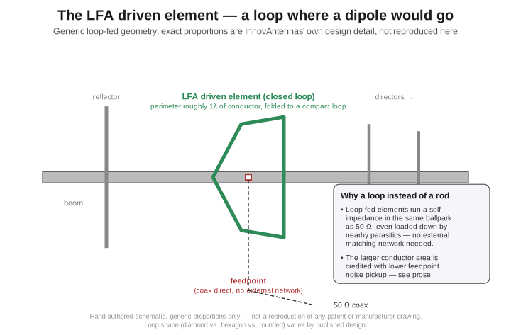
What is genuinely well-supported is the electrical mechanism, and it is a real answer to this volume’s central problem. A loop’s self-impedance, viewed at its own feed gap, tends to run in the same rough neighborhood as 50 Ω to begin with — the classic full-wave loop’s free-space feedpoint resistance is commonly cited in the 100–130 Ω range, comfortably higher than a half-wave dipole’s 73 Ω — and because the loop presents more conductor surface and a different current distribution than a thin rod, the same parasitic-loading mechanism of §2 pulls a loop’s feedpoint down from a higher starting point rather than from 73 Ω, which is enough in many designs to land it back in the neighborhood of 50 Ω without any external network at all. That is the electrical case for “no matching network needed” being defensible physics rather than only a marketing claim, independent of what the patent situation turns out to be. The mechanical cost is real too: a loop is a larger, more complex driven-element assembly than a split rod (more conductor, a bend or weld at each corner, more wind load), and it is one more reason the LFA shows up disproportionately on premium, EME-grade products rather than budget Yagis.
3.8 Four topology families: single-band, OWA, LFA, quagi
Pull the matching-scheme menu of §§3–7 back a level and it sorts into four design philosophies, each optimizing a different objective at the expense of the others.
Single-band traditional is the oldest and simplest philosophy: choose element lengths and spacings purely to maximize gain (or F/B) at one design frequency, accept whatever feedpoint impedance and bandwidth fall out, and match it with whichever scheme in §§4–6 fits the resulting number. This is the Cushcraft/Wilson/Hy-Gain-era approach, and it remains entirely valid where the operating requirement really is narrowband — a single CW/SSB segment, a fixed repeater-access frequency, a contest band where retuning between modes is not a concern. Its bandwidth, developed in §9, is the narrowest of the four families, which is the direct price of optimizing everything else without a bandwidth constraint in the mix.
OWA — Optimized Wideband Antenna — adds bandwidth explicitly as an optimization target alongside gain and F/B, rather than accepting whatever the gain-first design happens to produce. The technique originates with Prof. Jim Breakall, WA3FET, at Penn State University, using NEC-based numerical optimization across the whole design (element lengths and spacings jointly, not just the feed-cell spacing) to flatten the impedance and pattern behavior across a wider frequency range than a gain-first design would tolerate — this is a general antenna-engineering technique that predates and was subsequently adopted by M2 Antennas and other manufacturers, not something any single commercial vendor invented, and it is worth correcting that attribution explicitly since M2’s association with the term is common enough to be mistaken for its origin. The mechanism is not simply “space the elements farther apart” — it is a joint numerical optimization that typically detunes elements slightly off their individual gain-optimal lengths and adjusts spacing in tandem, trading a modest (roughly half a decibel to a full decibel) peak-gain sacrifice for a substantially flatter SWR and pattern across the band. Some current high-end designs go further still, combining OWA-style spacing optimization with an LFA-style loop driven element in the same product — sometimes marketed as “Advanced OWA” or similar hybrid naming — which is a reminder that these four families are design philosophies that blend in practice more than the clean categorical split suggests.
LFA, per §7, adds the loop-fed driven element’s naturally-closer-to-50-Ω self-impedance to the mix, most often (in current InnovAntennas products) paired with its own OWA-influenced spacing optimization rather than deployed on a bare gain-first design — so a “pure LFA vs. pure OWA” comparison somewhat understates how much the two philosophies already overlap in the current commercial catalog.
The quagi (quad-Yagi) predates both OWA and LFA and solves a related but distinct problem: replace the driven element with a square or diamond quad loop (rather than the LFA’s more elaborate proprietary loop shape) to get a cleaner, marginally better F/B than a plain dipole-driven Yagi, at the mechanical cost of spreaders and tensioning hardware the loop needs to hold its shape. Quagis had their strongest amateur following in 144/432 MHz EME work through the 1990s and 2000s, precisely the niche the LFA has since taken over for much the same electrical reason (a loop-type driven element behaving better under heavy parasitic loading) with a more refined, purpose-optimized geometry. The honest summary across all four: single-band traditional buys the most gain per element for the narrowest bandwidth and the least matching-network cost headache; OWA buys usable bandwidth at a modest, well-quantified gain cost; LFA adds a proprietary loop driven element’s natural-Z convenience on top of an OWA-adjacent spacing philosophy, at a mechanical cost and with a narrower commercial base than the conventional matches; and the quagi is largely a historical stepping stone that the LFA has displaced in its own strongest niche without displacing conventional matching everywhere else.
3.9 Bandwidth and the SWR curve — the 2 m vs. 6 m consequence
Vol 2 already established the array-level tradeoff — tighter element spacing and more directors buy gain and F/B at the cost of pattern and impedance bandwidth, the same mutual-coupling mechanism §2 traced through to the feedpoint. This section closes the loop specifically on what that narrowing looks like as an SWR-vs-frequency curve, and what it means for an operator choosing a topology for a real amateur band.
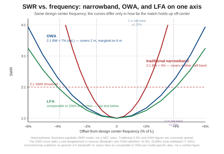
The commonly-quoted 2:1 SWR bandwidth figures are, once again, best treated as representative of a design philosophy rather than a fixed law: traditional single-band designs run roughly 3–5% of the design center frequency, narrowing further (toward 2%) on the longest, most tightly-coupled EME-class booms exactly where §2’s Q argument says the matching network is working hardest. OWA bandwidth is a genuinely contested figure across sources — Breakall’s own original OWA papers describe bandwidth improvements in the neighborhood of 4–5%, while separately-documented DL6WU-style wide-spaced designs (a related but distinct wideband philosophy, §2) reach 7–10%; the commonly repeated “8–12% for OWA” figure appears to conflate the two traditions, and this volume presents the OWA curve in the figure above as a middle estimate (≈ 7%) rather than endorse either extreme. LFA’s bandwidth is the least well-documented of the three: InnovAntennas’ published material gives specific SWR figures for specific models (for example, sub-1.3:1 or sub-1.4:1 SWR across a stated frequency span on particular 6 m products) rather than a general percentage-bandwidth claim applicable to the whole product line, so the LFA curve in the figure is drawn as comparable to OWA on the strength of those model-specific numbers rather than as a verified general figure — treat any single percentage attached to “LFA bandwidth” in secondary sources with real skepticism until it is traced to a specific model’s published sweep.
The practical consequence is where this section earns its place next to Vol 2 rather than inside it. A 2 m operator working the amateur allocation from 144 to 148 MHz needs the antenna to stay under 2:1 SWR across a 4 MHz span centered near 146 MHz — 4/146 ≈ 2.7% of band center, comfortably under 3%. A traditional narrowband design’s 3–5% bandwidth covers that span with room to spare, which is exactly why the classic single-band Yagi has never needed to apologize for its narrowband optimization on 2 m: the band itself is narrow enough that “narrowband” was never really a constraint in practice. A 6 m operator working 50 to 54 MHz needs coverage across a 4 MHz span centered on 52 MHz — 4/52 ≈ 7.7% of band center, roughly three times the 2 m figure in percentage terms, because 6 m’s absolute 4 MHz allocation is stretched across a much lower center frequency. A traditional 3–5% design does not reliably cover that whole span without retuning between the CW/digital end and the FM/repeater end of the band; this is precisely the situation an OWA or LFA design earns its keep in, and it is the reason 6 m in particular is where the wideband topologies show up disproportionately often in the commercial catalog, while a 2 m operator can reasonably stick with the simpler, cheaper, higher-peak-gain traditional design and never notice the difference.
It is worth being explicit about why the 6 m case is structurally different rather than just numerically different, because the reason is the same mutual-impedance mechanism §2 built the whole volume around, applied at a different absolute frequency. The 4 MHz of amateur allocation on both bands is an accident of spectrum regulation, not of antenna physics — but a Yagi’s electrical bandwidth scales with the fractional bandwidth its geometry supports, and a 6 m Yagi’s elements, being roughly three times longer than a 2 m Yagi’s for the same number of wavelengths of boom, see a proportionally identical fractional detuning across that same absolute 4 MHz. There is no design trick that makes a 6 m Yagi’s absolute megahertz-bandwidth larger without changing its fractional bandwidth; the only lever available is the fractional-bandwidth lever §8 already covers — loosen the feed-cell coupling (OWA) or swap in a loop driven element with a more forgiving self-impedance (LFA) — which is exactly why the wideband topologies concentrate on 6 m and above rather than being a uniform recommendation across the whole VHF/UHF range. A 70 cm (420–450 MHz) operator, working a 30 MHz allocation on a roughly 435 MHz center — about 6.9% — sits in almost the same boat as 6 m for this same reason, and sees the identical practical push toward OWA or LFA designs for full-band coverage.
3.10 Where this volume hands off
This volume traced the feedpoint from physics to hardware to design family. The impedance collapse below the free-space 73 Ω is the same mutual-coupling mechanism that produces a Yagi’s gain, read off the driven element’s own terminals rather than the far field — Z_in = Z_11 − Σ(Z_1k·Z_k1)/Z_kk, every parasitic element subtracting a further positive term, with the magnitude of the drop set by how tightly the feed cell is coupled (K1FO-style close spacing driving down toward 15–17 Ω even on long booms; DL6WU-style wide spacing holding near 50–60 Ω past twenty elements) rather than by element count alone. That same coupling made a longer, higher-gain array harder to match, quantified through a simple L-network Q argument that scales roughly as √(50/R_feed − 1) and directly costs a growing fraction of the marginal gain a long boom buys. The matching menu — direct feed (when the design lands near 50 Ω on its own), the folded-dipole 4:1 step-up (compounding usefully with parasitic loading rather than only undoing the free-space 73 Ω), the gamma match (flexible, field-tunable, weather-vulnerable, mildly pattern-asymmetric), the hairpin match (a single shunt inductor whose susceptance-cancellation is the same action as its resistance step-up — not two separate mechanisms), the T-match (the gamma’s symmetric, doubled-hardware sibling), and the LFA loop (a naturally higher-self-impedance driven element, correctly attributed here as a well-regarded, patent-pending design dating to roughly 2009–2010, originated by one manufacturer and since licensed to another and strongest in EME/weak-signal work — not a 2005-patented industry default) — covers the practical options a builder chooses among. Sorting those options into single-band traditional, OWA, LFA, and quagi families showed each optimizing a different objective (peak gain, bandwidth, natural match, loop-cleaned pattern) at a cost to the others, with real convergence between OWA and LFA in current commercial products. And the SWR-bandwidth picture closed the loop on why a 2 m operator has never needed to think about topology bandwidth (a 2.7% band fits comfortably inside even a narrowband design) while a 6 m operator, working a band that is 7.7% wide in percentage terms, genuinely needs the OWA or LFA answer.
The story continues into the hardware itself. Vol 4 takes the feedpoint-and-matching menu this volume built and puts it on a bench: a real bill of materials for a build using one of the matching schemes developed here, the tuning workflow with a NanoVNA that turns a hairpin’s or gamma’s two geometric degrees of freedom into a flat SWR sweep, the ranked commercial-buy survey across the topology families of §8, companion gear, and the common gotchas and myths that follow directly from getting a matching network’s mechanism wrong — most of them traceable straight back to the “the hairpin just cancels reactance” oversimplification §5 corrected here.
3.11 Resources
- ARRL Antenna Book (25th+ ed.), the Yagi and coupled-antenna chapters — the canonical amateur reference for mutual-impedance-driven feedpoint behavior and the standard matching-network topologies.
- Balanis, Antenna Theory: Analysis and Design (4th ed.) — the academic treatment of coupled-antenna mutual impedance and the
Z_in = Z_11 − Σ(Z_1k·Z_k1)/Z_kkrelation this volume’s §2 leans on. - Kraus, Antennas — the classic treatment of parasitic-array coupling and driven-element impedance behavior.
- Stutzman & Thiele, Antenna Theory and Design (3rd ed.) — complementary treatment of Yagi feed impedance and matching-network design.
- Sevick, Transmission Line Transformers (5th ed.) — the reference for the folded-dipole step-up and the transmission-line-transformer theory behind the choke baluns every matching scheme in this volume still needs; developed in full in the hub’s BALUNs & UNUNs dive.
- Cebik (W4RNL), published Yagi analyses — the source for the DL6WU-family measured feedpoint data (12/19/26-element 432 MHz figures) cited in §2, and for general Yagi feedpoint-impedance modeling discussion.
- Breakall (WA3FET), Penn State University — the original development of the Optimized Wideband Antenna (OWA) technique via NEC-based numerical optimization, later adopted industry-wide.
- G0KSC / InnovAntennas published material — the primary source for the LFA design’s own description of its patent-pending status and design history; treated in this volume with the hedges §7 documents rather than at face value.
- DL6WU (Günter Hoch) and K1FO (Steve Powlishen) design notes — the two contrasting long-boom feed-cell traditions cited in §2’s impedance-vs-element-count discussion.
- 4nec2 / EZNEC / MMANA-GAL (antenna modeling software dive) — the NEC-based tools that turn a target feedpoint impedance and matching-network geometry into a verified design before metal is cut.
Comments (0)