Yagi-Uda Antennas · Volume 1
The Parasitic-Array Principle — How a Passive Conductor Steers Radiation
The 1926 Tohoku work, correctly attributed; the reactance-to-current-phase derivation that turns a bare conductor into a reflector or a director; the mutual-impedance vector sum behind the forward lobe and rear null; and why a Yagi's geometry is its only tuning step
1.1 About this volume
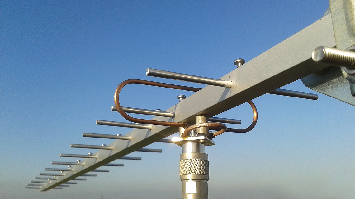
A Yagi-Uda beam looks like the simplest antenna in this entire hub — a driven element and a handful of unconnected rods bolted to a boom, no coils, no capacitors, nothing that moves. That simplicity is a disguise. Every rod on the boom except the fed one is doing genuine electromagnetic work with no wire running to it at all: each parasitic element is an independent, unfed oscillator, driven purely by the field its neighbors radiate, and the antenna’s entire directional personality — the forward gain, the deep rearward null, the feedpoint impedance collapsing to a fraction of the free-space 73 Ω — is a direct consequence of how that induced current’s phase lines up with the driven element’s own radiation. Get the phase story exactly right, in the rigorous sense of being able to derive the sign of an effect rather than just quote it, and the rest of the Yagi literature — which is mostly geometry tables — reads as a catalogue of consequences instead of a list of rules to memorize.
This volume owns exactly that phase story, and stops there deliberately. It covers the 1926 Tohoku Imperial University origin of the parasitic-array principle and — because the popular telling of that history compresses a more interesting truth into a slogan — takes the attribution seriously enough to check it against the historical record rather than repeat the slogan. It derives, from the coupled-circuit relationship every antenna text uses for parasitic arrays, exactly why an element cut longer than resonance behaves as a reflector and one cut shorter behaves as a director: what the reactance sign does to the induced current’s phase, and how that phase combines with the purely geometric path-length phase from the element’s spacing to produce constructive interference forward and destructive interference aft. It works through the three element roles — reflector, driven, director — in enough depth to explain why one reflector is nearly always sufficient, why parasitic loading collapses the driven element’s feedpoint impedance well below 73 Ω, and why each successive director buys less gain than the last. It resolves, against a real source rather than by picking a number, a genuine contradiction in the migrated chapter this volume replaces over how much shorter a fat element needs to be. And it closes by explaining why a correctly-built Yagi has no field-tuning step at all — the geometry is the tuning, for better and for worse.
What this volume does not cover, because later volumes own it, is the practical design space: the boom-length-versus-gain curve and the gain/bandwidth/front-to-back three-way tradeoff that decides how many elements to build (Vol 2); the actual matching networks — gamma, hairpin, T-match, and the loop-fed (LFA) driven element — that solve the low-impedance problem this volume only identifies and quantifies the size of (Vol 3); the radiation pattern, SWR curve, best- and worst-case deployment, and power handling (Vol 4); and the DIY build, commercial buys, and companion gear — rotator, mast, coax — that turn the principle into a physical antenna on a roof (Vol 5). Everything downstream of this volume assumes the reader already has the phase and impedance story straight; that is the entire point of putting it first.
1.2 The 1926 Tohoku work — getting the attribution right
The name on the antenna is “Yagi-Uda,” and the hyphen carries real information that the casual shorthand — “the Yagi antenna” — erases. The popular corrective to that shorthand, repeated often enough in amateur-radio circles to have become its own folk version, runs roughly: Uda did the actual research, and Yagi took the English-language credit. That version is closer to the truth than the shorthand it corrects, but it overshoots in the opposite direction, and the real history is more interesting than either simplification.
The experimental groundwork was Shintaro Uda’s. In 1925, working at Tohoku Imperial University in Sendai, Uda measured the effect that makes this whole antenna family possible — that a sharply directional beam could be formed from a driven element surrounded by accurately-spaced parasitic conductors — and presented those results in a report to the Institute of Electrical Engineers of Japan. That first report was in Japanese only, with no detailed description reaching an English-reading audience. If the story stopped there, the folk version would be exactly right: Uda alone had the antenna, and no one outside Japan knew it existed.
It does not stop there, and this is the detail the folk version drops. The following year, 1926, Yagi and Uda jointly published the paper that gave the antenna its first detailed English-language description — geometry, characteristics, the parasitic-array mechanism — in the Proceedings of the Imperial Academy of Japan, under a title usually rendered in English as “Projector of the Sharpest Beam of Electric Waves.” This is the paper this volume, and every citation to “the 1926 Yagi-Uda work,” actually refers to, and it was co-authored, not ghost-written. Hidetsugu Yagi was Uda’s supervisor at Tohoku, and by every account he credited Uda’s originating experimental work; the 1926 paper’s joint authorship reflects a real collaboration, not a senior name attached after the fact to a junior colleague’s unread results.
What actually skews the credit toward Yagi alone happened two years later. In 1928, Yagi — by then with substantial international experience from time in the UK, Europe, and the United States — published a solo-authored paper in the Proceedings of the IRE (the predecessor of the IEEE, and at the time the most widely read English-language radio-engineering journal in the world). That paper is what actually carried the parasitic-array principle to American and European radio engineers; it is the publication that triggered the wave of international interest in directive UHF antennas, and it is the reason the antenna picked up “Yagi” as its common single-word name in English-speaking countries. The asymmetry compounds at the patent office, though not in the direction the tidy version of the story suggests: the Japanese patent was filed under Yagi’s name alone, without Uda’s on it, and was later transferred to the Marconi Company in the UK; the United States patent (1,860,123, issued 1932) was assigned not to Yagi personally but to the Radio Corporation of America. So the paperwork asymmetry is real, but it is Yagi-without-Uda on the Japanese filing and a corporate assignee on the American one — not, as is sometimes written, a joint Japanese patent and a solo American one. A version of the folk story sharper than the shorthand but no less compressed — “Yagi patented what Uda invented” — is also not quite right, because Yagi’s own writing on the subject is consistent in crediting Uda’s principal contribution; what happened is closer to an international-visibility and paperwork asymmetry than a deliberate erasure.
The honest one-paragraph version, then: Uda ran the defining experiments and reported first, in Japanese, in 1925. The pivotal English-language paper that actually described the antenna to the world — the one this volume’s “1926 Yagi-Uda paper” citation means — was a genuine joint publication the following year. Yagi’s further, solo 1928 paper in a major international journal, combined with a US patent filed under his name only, is what tilted the antenna’s common name toward him specifically, over Uda’s explicit objection to nothing — by all accounts Yagi never claimed sole credit and the “Yagi-Uda” naming that persists in the engineering literature is the field’s own correction of the popular shorthand, not a recent revisionist relabeling. This account is drawn from historical-review secondary sources rather than a direct reading of the 1925/1926/1928 papers themselves (the earliest is in Japanese and the later two are in period journals this volume has not examined firsthand), and the reader should treat the fine details — exact wording of titles, the precise content Uda’s 1925 report covered — as consistent across the sources checked but not independently verified against the primary documents.
1.3 Reactance, current phase, and the reflector/director sign convention
Every Yagi text states the rule the same way: an element cut longer than a half-wave is inductive and behaves as a reflector; one cut shorter is capacitive and behaves as a director. Almost none of them derive it, and the gap between stating a sign convention and deriving one is exactly where hand-waving lives. It is worth closing that gap explicitly, because the derivation is short and it is the same derivation that explains every other quantitative claim in this volume.
Treat the driven element and a single parasitic element as a coupled two-port circuit — the same formalism used for any pair of mutually-coupled resonators, borrowed directly into antenna theory (Kraus, Antennas; Balanis, Antenna Theory, both devote a full treatment to it for parallel dipoles). Terminal voltage and current at the two elements obey
V₁ = I₁·Z₁₁ + I₂·Z₁₂ and V₂ = I₁·Z₂₁ + I₂·Z₂₂,
where Z₁₁ and Z₂₂ are the driven and parasitic elements’ own self-impedances (radiation resistance plus whatever reactance their length away from self-resonance contributes) and Z₁₂ = Z₂₁ = Z_m is the mutual impedance the two elements’ near fields induce between them — a complex, spacing-dependent quantity that is not something you would want to hand-derive for an arbitrary geometry, but that is tabulated for parallel dipoles in every serious antenna reference (Kraus’s mutual-impedance-versus-spacing curves for parallel dipoles are the classic version; both the real and imaginary parts of Z_m oscillate with spacing, and both matter). The driven element has a source, so V₁ ≠ 0. The parasitic element has none — it is a single unbroken length of tubing, which electrically is the same statement as “the voltage across an imagined gap at its center is zero,” V₂ = 0. Substituting into the second equation and solving,
I₂ = −I₁ · (Z_m / Z₂₂),
with Z₂₂ = R₂₂ + jX₂, R₂₂ the parasitic element’s own radiation resistance and X₂ the reactance its physical length contributes relative to its own self-resonant length. This one line is the whole physics of a parasitic element, and it is worth sitting with because it is exactly where most treatments stop deriving and start asserting.
Cut the parasitic element to its own exact self-resonance — X₂ = 0 — and I₂ = −I₁·(Z_m/R₂₂). To the extent Z_m is dominated by its real part at the chosen spacing, this is very nearly a real multiple of I₁: close to in phase with the driven current, or close to 180° out of phase, with little of the quadrature that end-fire operation needs. That qualifier is doing real work and should not be dropped, because Z_m is itself complex — its reactive part does not vanish just because the parasitic element’s own reactance has. So a resonant parasitic is not rigorously confined to the driven element’s phase axis; some phase offset is already present through Im(Z_m), and the honest statement is that resonance removes the large, deliberately controllable phase term (X₂) while leaving a smaller residual one set by the geometry. What remains true, and is the point worth carrying forward, is that a parasitic element cut exactly to resonance gives the designer no useful phase lever, and an array with every element at resonance is not a beam — which is the precise, derivable reason a Yagi with every element cut exactly to resonance is not a beam, and it is also the derivation behind the flat statement every Yagi text repeats (“a resonant parasitic re-radiates in phase”) without saying why that fact matters.
Detune the element off resonance and X₂ stops being zero, and dividing I₁·Z_m by (R₂₂ + jX₂) instead of R₂₂ alone rotates I₂’s phase in the complex plane. Lengthen the element past resonance — which for a fixed operating frequency means the element is now electrically below its own self-resonant frequency, exactly the same “longer-than-resonant is inductive” relationship the single-band dipole dive establishes for a dipole detuned by frequency at fixed length rather than by length at fixed frequency — and X₂ becomes positive. Dividing a fixed-phase source term by a denominator whose imaginary part has grown positive is the identical operation as driving a series R-L branch above its own resonance: the resulting current lags the source. Shorten the element past resonance and X₂ goes negative — capacitive — and the same division rotates the current the other way: it leads. This is not a lumped-circuit metaphor borrowed to make the antenna case intuitive; Z₂₂ = R₂₂ + jX₂ is the literal complex impedance the parasitic element presents at its own (imaginary) terminals, and the current-phase behavior follows the same AC-circuit algebra a series RLC branch obeys because it is that algebra, applied to a radiating structure instead of a lumped one. The dipole dive’s frequency-domain detuning and this volume’s length-domain detuning are two different ways of sweeping the identical underlying reactance — one holds physical length fixed and sweeps frequency, the other holds frequency fixed and sweeps length — and both rotate the current-phase dial in the same direction for the same reason.
Current phase alone does not produce a directional pattern. A phase offset between two otherwise-identical radiators is, by symmetry, indistinguishable in the forward and backward end-fire directions unless something else breaks that symmetry — and the something else is a second, purely geometric phase term. A wave launched from an element spaced a distance s behind the driven element has farther to travel to reach a distant observer in front of the array than a wave from the driven element itself has, and correspondingly less far to travel to reach an observer behind the array. In array-factor notation this extra path length contributes a term e^{jks·cosθ} to the parasitic’s far-field contribution, where θ is measured from the array’s forward axis and k = 2π/λ. Evaluate that term at θ = 0° (dead ahead) and at θ = 180° (dead astern) and its sign flips — the identical physical spacing produces a phase advance in one direction and an equal phase delay in the other, which is the symmetry-breaking ingredient current phase by itself cannot supply.
A Yagi’s directionality is the sum of exactly these two phase terms, chosen by the designer to land on a specific combination: reactance-driven current phase (set by how far off resonance the element is cut) plus geometry-driven path phase (set by how far it is spaced), summing to something close to zero net phase difference in the forward direction — reinforcing the driven element’s own radiation — and something close to 180° in the backward direction — canceling it. A longer, inductively-detuned element placed behind the driven element supplies a lagging current that, combined with a position where the geometric term already favors a forward-direction phase advance, reinforces forward and opposes rearward: a reflector. A shorter, capacitively-detuned element placed ahead of the driven element supplies a leading current that does the identical job from the front: a director. Every subsequent director keeps leading progressively more (§7) precisely because each one sits farther forward, where the geometric term demands progressively more current-side compensation to keep landing near the same forward-constructive alignment.
This is the derived version of “longer is a reflector, shorter is a director” — reactance sign, current-phase rotation, geometric path-phase, forward reinforcement, rearward cancellation, each step a specific consequence of I₂ = −I₁·Z_m/Z₂₂ rather than an assertion. What it deliberately does not give you is the exact numerical current amplitude and phase at a specific spacing and detuning: Z_m is a transcendental function of spacing with real and imaginary parts that do not reduce to a hand-friendly closed form, which is exactly why NEC-2/NEC-4 modeling — its own sub-project elsewhere in this hub — exists: it solves this same relationship numerically, generalized to every element pair simultaneously, for whatever geometry it is given. Figure “Reflector and director currents, phased forward and canceled aft” sketches the resulting picture — a reflector’s current lagging, a director’s leading, and the two directions’ geometric terms turning that into forward addition and rearward cancellation — with representative rather than NEC-derived angles, because the exact values are a function of the spacing actually chosen, not a fixed constant of the topology.

1.4 The mutual-impedance picture — vector summation and the spacing-phase tradeoff
Extend §3’s two-element relationship to a full Yagi and the picture generalizes directly: every parasitic element’s current is set by the same driven-element field, mediated by its own mutual impedance to the driven element (and, in a full treatment, by mutual coupling to every other parasitic element too — a detail NEC handles as a matter of course and hand analysis mostly ignores as a second-order correction). The far field in any direction is the vector sum of each element’s current, each carrying its own reactance-driven phase from §3 plus its own geometry-driven path phase from its position along the boom. Figure “A representative 5-element 144.1 MHz Yagi — geometry” lays out a representative geometry to make the rest of this section concrete: a reflector 5.0% longer than the driven element spaced 0.20λ behind it, a driven element at 990 mm, and three directors at −4.0%, −6.1%, and −8.1% relative to the driven element, spaced 0.15λ, 0.20λ, and 0.25λ apart respectively — spacing that grows toward the tip, for reasons §7 makes quantitative. This is an illustrative geometry chosen to be internally consistent with the numbers in this volume, not a construction template; a build-ready design is Vol 5’s job. One number in it is worth flagging so it does not read as a contradiction later: those spacings sum to a boom of roughly 0.8λ, while Vol 2’s gain tables use ~1.0λ as the representative figure for a 5-element design. Both are legitimate — boom length for a given element count is a design choice, not a fixed property of the count, and the spread between a compact 5-element and a stretched one is exactly the tradeoff surface §6 describes. Neither number should be read as the 5-element boom length.

The reason spacing and detuning trade against each other follows directly from §3’s two phase terms adding to a target total. The reactance term contributed by an element’s own detuning and the geometric term contributed by its spacing are, to good approximation, independent knobs that both move the same final quantity — the parasitic’s effective phase as seen in the forward direction. That means the same net forward-alignment result is reachable by more than one combination: a reflector cut further from resonance (more inductive reactance, larger current-phase lag) at closer spacing, or a reflector cut closer to resonance (less reactance, smaller lag) at wider spacing, because the wider spacing supplies more of the needed phase shift through the geometric term instead. This is precisely why every published Yagi design pairs a specific detuning percentage with a specific spacing rather than either dimension alone — Günter Hoch’s DL6WU designs, Steve Powlishen’s (K1FO) designs, and Justin Johnson’s (G0KSC) LFA series each represent a different point on that same tradeoff surface, optimized for different objectives (peak gain, side-lobe suppression, bandwidth), and Vol 2 is where those named design traditions and the boom-length-versus-gain curve they trace out get the depth they deserve.
The tradeoff has a practical floor and ceiling worth naming here even though the design-space exploration itself belongs to Vol 2. Spacing an element too close to the driven element (under roughly 0.1λ) drives the mutual resistance term R_m toward the same order of magnitude as the parasitic’s own radiation resistance, which makes the element’s behavior extremely sensitive to small length errors — a fraction-of-a-percent cutting mistake shifts X₂ enough to noticeably rotate the current phase and detune the whole array’s forward alignment. Spacing it too far (beyond roughly 0.3–0.4λ for a reflector, further still for directors deep in a long boom) weakens the mutual coupling Z_m enough that the induced current becomes too small to contribute meaningfully regardless of how well its phase is chosen — the element becomes electromagnetically present but functionally decorative. The practical spacing range every published design lands in, roughly 0.1–0.35λ element-to-element, is the band where mutual coupling is strong enough to matter and forgiving enough that ordinary construction tolerances do not wreck the phasing — not an arbitrary convention.
1.5 The reflector — why one is (almost) always enough
A reflector is a single parasitic element placed behind the driven element, in the direction opposite the desired beam, cut longer than the driven element’s resonant length so that §3’s derivation gives it a lagging current relative to the driven element. The standard figure — roughly 5% longer than the driven element at a spacing in the 0.15–0.25λ range — is not an arbitrary round number so much as a point on the tradeoff surface §4 describes that a great deal of published NEC modeling has converged on as a good compromise between forward gain, front-to-back ratio, and how sensitive the result is to small construction errors.
The question that actually needs answering, rather than merely asserting, is why a second reflector — one placed still further behind the first — buys so little. The reason follows from the same mutual-impedance relationship: a reflector’s contribution to the forward field scales with the strength of its coupling to the driven element, Z_m, which falls off with distance (not monotonically — the mutual-impedance curves for parallel dipoles oscillate rather than decay smoothly — but the envelope trends downward as spacing grows). A second reflector, positioned still farther back to avoid crowding the first, sits at a spacing where its coupling to the driven element is already considerably weaker than the first reflector’s, so the current it can have induced in it — no matter how well-phased — is smaller to begin with, and its resulting contribution to the forward field is smaller still. NEC-modeling literature on double-reflector Yagis (Cebik’s published modeling work and the ARRL Antenna Book’s Yagi chapter both discuss the case) consistently reports the improvement as well under a decibel, commonly cited in the range of a few tenths of a dB — a genuine but marginal gain purchased at real mechanical cost (another element, another spacing to get right, more boom length and wind load) and often at a small bandwidth or beamwidth penalty from the added rearward structure. This is a reported empirical result from repeated modeling rather than a number this volume derives from first principles; the qualitative reason it should be small — weaker coupling at greater distance, on top of a diminishing-returns curve that is already steep for parasitic elements generally (§7 quantifies the same effect for directors) — is the derivable part, and it is why essentially every published Yagi design, from a 3-element portable design to a 20-element EME monster, uses exactly one reflector rather than two.
1.6 The driven element — parasitic loading and the impedance collapse
The driven element is the antenna’s only fed component, and its role sounds deceptively like a plain half-wave dipole’s: cut to resonance, present a real feedpoint impedance, accept a feedline. What actually happens at its terminals is more interesting, and it follows directly from the same coupled-circuit relationship §3 introduced — extended to include the driven element’s own equation rather than stopping at the parasitic’s.
Return to V₁ = I₁·Z₁₁ + I₂·Z₁₂ and solve for the impedance actually seen at the driven element’s terminals, Z_seen = V₁/I₁ = Z₁₁ + (I₂/I₁)·Z₁₂. Substituting §3’s result for the parasitic current, I₂/I₁ = −Z_m/Z₂₂ (using Z₁₂ = Z_m for the mutual term), gives
Z_seen = Z₁₁ − Z_m² / Z₂₂.
This is the standard driving-point-impedance relation for a driven element in the presence of a parasitic conductor (Kraus and Balanis both derive versions of it), and it says something specific and useful: the driven element’s own free-space self-impedance, Z₁₁ — the familiar 73 + j42.5 Ω the single-band dipole dive derives for an isolated half-wave element — gets a subtracted correction term whose size depends on how strongly the parasitic couples to the driven element (Z_m, spacing-dependent) and how the parasitic’s own detuning shapes its self-impedance (Z₂₂). Each additional parasitic element contributes its own such term, subtracted from the same starting Z₁₁ — but the size of any one element’s term is set by Z_m²/Z₂₂, and Z_m is a strong, spacing-dependent quantity, not a fixed per-element decrement. That distinction is the whole story: element count sets how many terms are in the sum, but spacing sets how large each term is, and a designer who deliberately widens the feed-cell spacing keeps every added director’s term small enough that the running total barely moves, however many directors follow. Feedpoint resistance therefore does not decline monotonically with element count in real designs — it tracks how tightly the feed cell is coupled, a spacing choice the designer makes, not the raw number of parasitic elements on the boom. Two published long-boom traditions make the point concretely, and Vol 3 works through the matching consequences of both: Steve Powlishen’s (K1FO) closely-spaced, side-lobe-optimized designs deliberately keep the feed-cell coupling tight, holding the driven-element resistance down around 15–17 Ω even on booms of twenty elements or more. Günter Hoch’s (DL6WU) wide-spaced tradition makes the opposite choice, loosening the feed-cell spacing specifically to keep each added director’s Z_m²/Z₂₂ term small; NEC-modeled 432 MHz designs in that tradition (Cebik/W4RNL’s published DL6WU-series analysis) show no systematic decline at all from 10 to 40 elements — 49.65 + j13.75 Ω at 10 elements, 57.93 + j10.14 Ω at 19, 51.42 + j3.80 Ω at 28 — oscillating in a rough 48–68 Ω band the whole way out rather than trending toward the teens. The subtraction in Z_seen = Z₁₁ − Z_m²/Z₂₂ is real and it is the entire mechanism behind both traditions, but it is a statement about coupling strength, not a countdown keyed to element count.
The consequence is a genuine engineering problem this volume is explicitly not solving: a feedpoint in the 15–35 Ω range is a poor match to 50 Ω coax on its own, and the driven element’s physical form — plain dipole, folded dipole (a 4× step-up before any external network), or the loop-fed (LFA) driven element that lands close to 50 Ω natively — is chosen specifically around which matching approach the rest of the design wants to use. Working out the gamma match, hairpin match, T-match, and LFA loop options that actually solve this collapsed impedance for a real feedline is Vol 3’s entire subject; what belongs here is only the derivation of why the collapse happens and roughly how far it goes, so that Vol 3’s matching discussion starts from a quantified problem rather than an assertion that “parasitic elements lower the impedance.”
1.7 The directors — progressive shortening and the diminishing-return curve
Directors sit forward of the driven element, each cut shorter than the last — a typical drop of 1–4% per element relative to its immediate neighbor — with spacing that grows from roughly 0.15λ nearest the driven element toward 0.30–0.40λ between the outermost pair on a long boom. Both trends follow directly from §3’s derivation and §4’s tradeoff: each successive director sits at a position where the geometric path-phase term already differs from its neighbor’s, so its required current-phase lead (and hence its required detuning) shifts accordingly, and the growing spacing partly compensates for weakening mutual coupling at greater distance from the driven element by asking less of the current-phase term at each step.
Figure “Current magnitude and phase across a 5-element array” sketches the qualitative shape this produces: current magnitude tapering from element to element moving out along the director chain (weaker coupling at greater spacing means a smaller induced current, regardless of how well its phase is chosen) while the current’s phase lead relative to the driven element continues to grow. This is a representative profile of the shape NEC modeling produces for a design in this size class, not measured data from a specific build — the exact numbers for any real design are whatever its own optimization run produces — but the trend (shrinking magnitude, growing phase lead, moving outward) is the derivable consequence of §3–§4’s mechanism applied element by element.

The gain contribution per director follows a steep diminishing-returns curve that every practical Yagi builder eventually runs into. Typical NEC-modeled figures across the common design traditions put the first director’s contribution at roughly +1.5 to +2.0 dB over a bare 2-element (reflector + driven) array, the second director at roughly +0.8 to +1.2 dB more, the third at +0.5 to +0.8 dB, and each director beyond the fourth or fifth contributing well under half a dB — figures that, again, should be read as typical and design-dependent rather than fixed constants, since the actual per-element contribution for any published design is whatever its own boom-length-versus-gain modeling produced. One caution before anyone reaches for a calculator: these are not summable increments. Vol 2 §2 chains them against the corrected gain-versus-boom curve and shows they do not reproduce it cleanly — matching at three elements, overshooting slightly at four, then undershooting by close to a full decibel by five to nine. Treat them as independent per-element estimates of a diminishing trend, not as a series to add up. The mechanism behind the diminishing curve is the same one §5 gave for a second reflector: each additional director sits farther from the driven element, where the mutual coupling that induces its current in the first place is weaker, so however well its phase is chosen the magnitude of what it contributes keeps shrinking. Most amateur Yagis stop at 5–9 elements for exactly this reason — the marginal gain per added element and per added foot of boom has already fallen well below what the added mechanical complexity, wind load, and cost are worth — while EME and other weak-signal specialties push to 15 elements or more per boom (and then stack multiple booms) because even a few tenths of a decibel matters when the signal is already near the noise floor. The full boom-length-versus-gain curve, the 3-dB-per-doubling rule that traces it, and the decision between a longer boom and a stacked array are Vol 2’s subject in depth; what belongs here is only the mechanism that makes the curve diminish in the first place.
1.8 Element diameter and the length correction it forces
Every element length quoted so far — the driven element’s resonant length, the reflector’s +5%, the directors’ progressive shortening — is stated relative to an idealized thin conductor. Real Yagi elements are aluminum tubing, often a substantial fraction of an inch or more in diameter, and diameter changes the physical length needed to reach a given electrical resonance. Getting the size of that correction right matters enough to be worth resolving carefully, because the migrated chapter this volume replaces states it two different ways in two different places — “fatter elements need 5–15% less length” in one section and “fatter elements need ~10–20% less length” in another — and neither number should be trusted as written.
The mechanism is the identical end-effect the single-band dipole dive derives for a plain wire dipole: a conductor’s open, high-voltage tip carries shunt (fringing) capacitance that is electrically equivalent to a small amount of extra length, and a fatter conductor concentrates more of that capacitance at the tip relative to its own length, so it must be trimmed physically shorter to reach the same electrical resonance a thinner conductor would reach at its full thin-wire length. That dive’s own trim-factor table is the concrete version of this fact: k (physical length as a fraction of the free-space half-wavelength) runs around 0.96–0.97 for thin HF wire and falls to roughly 0.92–0.93 for half-inch VHF tubing — a real, physically-grounded effect, but a total swing across that particular diameter range of only about 3–5%, nowhere near either of the migrated chapter’s numbers. The correction is not a fixed percentage at all; it is a monotonic function of the element’s length-to-diameter ratio ℓ/d (equivalently, of diameter relative to wavelength, d/λ), formalized in antenna theory through the “thickness parameter” Ω = 2·ln(2ℓ/d) that governs the classical thin-to-thick antenna current-distribution and length-correction curves (Balanis derives this version explicitly).
A concrete, independently-sourced number makes the scale of the effect clear for an actual amateur Yagi. L. B. Cebik (W4RNL), working through a 3-element 20-meter Yagi design in detail, computed the required reflector length at three tubing diameters — 0.5”, 1.0”, and 1.5” — and found the resonant length shrinking from 417.80” at 0.5” diameter to 414.72” at 1.0” and 413.12” at 1.5”: a 3× increase in diameter producing roughly a 1.1% reduction in length, not 10%, let alone 20%. That is a modest, HF-typical correction, and it is the number to trust for the aluminum-tubing diameters — a quarter-inch to an inch or so — that dominate HF and VHF amateur construction, where d/λ is small (on the order of 0.001–0.01).
The larger corrections do exist, but they live in a different regime than typical ham HF/VHF tubing, and conflating the two regimes is very likely how the migrated chapter’s contradictory numbers got there in the first place. NBS Technical Note 688 (Peter Viezbicke, 1976) — the definitive published source for optimized Yagi element dimensions, and the basis for the design curves the ARRL Antenna Book reproduces — establishes its baseline design at d/λ = 0.0085 and provides correction curves specifically because moving to a different diameter-to-wavelength ratio requires a different, non-constant correction rather than a fixed offset; there is no single percentage that covers every d/λ a builder might use. At the fat end of that curve — element diameters that are a meaningful fraction of a wavelength, the regime of UHF and microwave Yagis rather than HF or 2-meter designs — the correction grows well beyond the ~1% of the HF example above, and Viezbicke’s own curves, not a flat percentage, are what a builder should be reading off. It is worth being careful about which published measurements support which claim here, because this is exactly where the migrated chapter’s two contradictory numbers most likely came from. The frequently-cited VK2KU measurements are boom-diameter data — that experiment’s large 0.05–0.08 λ figures are boom-to-wavelength ratios, with its actual element diameters spanning only about 0.002–0.021 λ — so they belong to the second effect described below, not to the pure element-diameter correction being discussed here. Citing them for element diameter alone commits precisely the conflation this section exists to separate.
There is a second, genuinely separate effect worth distinguishing from element diameter alone, because folklore tends to merge the two: when an element passes through and bonds electrically to a metal boom (as opposed to simply being a fat conductor in isolation), the boom itself contributes its own additional shortening, on top of whatever the element’s own diameter already requires. Fletcher’s VK2KU measurements quantify this too — the boom forces the element’s near-field current to flow around the boom’s surface rather than directly along the element, reducing the stored magnetic energy near the element’s center and presenting a negative (shortening) reactance contribution that must be compensated by lengthening the element beyond its already-diameter-corrected length. This boom-coupling correction and the pure element-diameter correction are both real, both shorten the required physical length, and both scale with the relevant diameter-to-wavelength ratios rather than with a fixed percentage — but they are mechanistically distinct effects (fringing capacitance at the tip versus current displacement around a boom at the center), and a builder correcting for one without recognizing the other is solving half the problem. Neither correction is something to guess at with a flat percentage; NEC-2/NEC-4 modeling, the standard mechanical-insulator-versus-metal-boom design charts (Günter Hoch’s DL6WU corrections, reproduced in the VHF/UHF DX Book), or Fletcher’s own published boom-correction curves are the actual sources a builder should consult, and Vol 5’s DIY build works from exactly those rather than restating a single number here.
1.9 Why a Yagi has no field-tuning step
Every mechanism this volume has derived — the reactance-to-current-phase relationship, the mutual-impedance vector sum, the driven-element impedance collapse, the diameter and boom-coupling length corrections — has the same character: it is entirely a function of the antenna’s fixed physical geometry. Element lengths, element diameters, boom-relative electrical shortening, and spacings between elements are the complete list of inputs to every equation in §§3–8, and none of them is adjustable after the antenna is built without literally cutting metal. There is no trimmer capacitor, no sliding tap, no ferrite core to bias — no equivalent, anywhere on a properly designed Yagi, of the “adjust until it peaks” step that governs an L-network tuner or a variable-inductance loading coil elsewhere in this hub.
This is the sense in which the geometry is the tuning. Once the elements are cut to spec and mounted at the spec’d spacing, every quantity this volume has derived — the reflector’s lagging current and the directors’ leading currents, the forward-constructive/backward-destructive vector sum, the collapsed feedpoint resistance — is determined by physics, not by anything an operator does afterward. Build the geometry correctly and the antenna performs to its design; cut an element a few percent off, or crowd a spacing, and the current phases §3 derived shift enough to measurably degrade the forward gain and front-to-back ratio, with no field adjustment available to claw it back short of re-cutting the element. This is exactly why the high-end Yagi manufacturers (M2, Force 12, InnovAntennas among others) sell precision-machined elements with tight length and mounting tolerances rather than “close enough” stock — the tolerance budget lives entirely in the metal, because there is nowhere else for it to live.
The one genuinely adjustable part of a real Yagi installation is the matching network at the driven element’s feedpoint — the gamma capacitor’s tap position, the hairpin stub’s dimensions, or (for an LFA driven element) essentially nothing at all, because the loop geometry is designed to land close to 50 Ω without an adjustable network in the first place. That single adjustable degree of freedom exists because §6 established that the driven element’s impedance, after parasitic loading, sits well below the coax’s 50 Ω, and something has to bridge that specific gap — but the matching network only ever corrects the feedline transition, never the antenna’s radiation pattern or gain. A Yagi with a perfectly tuned gamma match and elements cut 3% short is a well-matched antenna radiating several dB below its design gain in the wrong direction on top of it; the SWR meter reading 1.2:1 tells you nothing about whether the geometry underneath it is correct. Solving that one remaining adjustable piece — what gamma, hairpin, T-match, and LFA-loop matching actually look like in practice — is Vol 3’s job in full.
1.10 Where this volume hands off
This volume derived the physics that every later Yagi volume in this dive builds on top of. It corrected the popular attribution folk tale against the historical record: Uda’s 1925 Japanese-only experiments established the effect, the pivotal English-language description was a genuine 1926 Yagi-Uda joint publication, and it was Yagi’s further, solo 1928 paper in the Proceedings of the IRE — plus a Japanese patent filed under his name alone, without Uda’s, and a US patent assigned to RCA — that skewed the antenna’s common name, not a case of Yagi silently taking credit for work he had no part in. It derived, from the coupled-circuit relationship I₂ = −I₁·Z_m/Z₂₂, exactly why an inductively-detuned (longer) element’s current lags and a capacitively-detuned (shorter) element’s current leads, and how that current-phase term combines with the purely geometric spacing-phase term to produce a Yagi’s forward-constructive, backward-destructive interference pattern — the rigorous version of “longer is a reflector, shorter is a director” rather than the asserted one. From the same relationship it derived why one reflector is nearly always enough (weaker coupling at greater distance, on top of an already-steep diminishing-returns curve), why the driven element’s feedpoint impedance collapses well below 73 Ω as more parasitic elements are added (Z_seen = Z₁₁ − Z_m²/Z₂₂, one subtracted term per parasitic element), and why each successive director buys less gain than the last. It resolved the migrated chapter’s own internal contradiction over element-diameter length correction against real sources — Cebik’s ~1.1% HF example, the NBS TN688 baseline and correction-curve framework, and Fletcher’s (VK2KU) boom-and-diameter measurements at VHF/UHF/microwave — landing on “it depends on ℓ/d, and it is much smaller for typical ham tubing than either of the migrated chapter’s flat percentages claimed” rather than a single number. And it closed by establishing why none of this is field-adjustable except the feedpoint match: the geometry is the tuning, for exactly the reasons the physics in §§3–8 makes explicit.
The story continues from here into the practical design space this volume deliberately did not enter. Vol 2 takes the diminishing-returns curve §7 introduced and works out the full boom-length-versus-gain relationship, the front-to-back and bandwidth tradeoffs that pull against peak gain, and the named design traditions — DL6WU, K1FO, G0KSC’s LFA, OWA wideband designs — that occupy different points on that tradeoff surface. Vol 3 takes the collapsed feedpoint impedance §6 quantified and works through the actual matching solutions: gamma, hairpin, T-match, and the loop-fed driven element that sidesteps the problem by design. Vol 4 develops the radiation pattern, HPBW, SWR-versus-frequency behavior, and the best-case and worst-case deployment scenarios this volume’s geometry produces, along with power-handling limits. Vol 5 puts all of it into a real, buildable design: a bill of materials with actual part numbers, the step-by-step construction and NanoVNA tuning workflow, a ranked commercial-buy survey, and the rotator/mast/coax companion gear a Yagi installation actually needs.
1.11 Resources
- Yagi, H. and Uda, S., “Projector of the Sharpest Beam of Electric Waves” (1926), Proceedings of the Imperial Academy of Japan — the joint publication that first described the parasitic-array antenna in English; the paper this volume’s “1926 Yagi-Uda work” refers to.
- Yagi, H. (1928), Proceedings of the Institute of Radio Engineers — Yagi’s solo paper that carried the principle to American and European radio engineers and is largely responsible for the antenna’s common “Yagi” name in English.
- ARRL Antenna Book (25th+ ed.), the Yagi-Uda chapter — the canonical amateur reference; reproduces the NBS-derived element-diameter design curves this volume discusses in §8.
- Kraus, J. D., Antennas — the classic derivation of parasitic-array mutual impedance, the two-parallel-dipole mutual-impedance curves used in §3–§4, and the driving-point-impedance-in-the-presence-of-parasitics relation used in §6.
- Balanis, C. A., Antenna Theory: Analysis and Design (4th ed.) — the academic treatment of parasitic arrays, mutual coupling, and the thickness-parameter (
Ω = 2ln(2ℓ/d)) length-correction theory used in §8. - Viezbicke, P. P., “Yagi Antenna Design,” NBS Technical Note 688 (1976) — the definitive published Yagi design-curve source, including the
d/λ = 0.0085baseline and diameter-correction curves discussed in §8. - Cebik, L. B. (W4RNL), “Yagi Element Diameter Differences Do Make a Difference” — the worked 3-element 20 m example (0.5”–1.5” tubing) this volume’s §8 cites directly.
- Fletcher, G. (VK2KU), “Effects of Boom and Element Diameters on Yagi Element Lengths at 144, 432 and 1296 MHz,” QEX, Jan/Feb 2000 — the experimental boom- and element-diameter correction data used in §8.
- Hoch, G. (DL6WU) boom-correction data, reproduced in The VHF/UHF DX Book (I. White, G3SEK, ed.) — the widely-used practical correction figures referenced in §8.
- 4nec2 / EZNEC / MMANA-GAL and the broader NEC-2/NEC-4 modeling toolchain (its own sub-project elsewhere in this hub) — the numerical tools that solve the coupled-circuit relationship in §3–§4 exactly, for any real geometry, rather than by the closed-form approximations this volume uses to derive the underlying mechanism.
Comments (0)