NanoVNA · Volume 1
What a Vector Network Analyser Actually Measures
The reflection coefficient Γ as the primitive quantity, SWR and return loss as its lossy derivatives, the 2-port S-parameter set and the reference-plane concept, the Γ↔Z↔Smith-chart mapping, and what the NanoVNA's bridge-mixer-synthesizer architecture buys and costs
1.1 About this volume
This volume is the one every other volume in this dive — and every “verify the build with a NanoVNA” pointer scattered across the rest of the Antennas hub — quietly assumes you already understand. Before any hardware survey, before a single calibration button-press, before the on-device Smith-chart mode or the host-software workflow, there is a prior question that determines whether any of that machinery means anything: what is the instrument actually measuring, and what does it throw away when it hands you a number?
The short answer is that a vector network analyser measures one thing — a complex ratio of two travelling waves at a defined reference plane — and every other number a NanoVNA displays (SWR, return loss, R + jX, a Smith-chart dot, an S21 trace in dB) is arithmetic performed on that one measurement after the fact. Get comfortable with that hierarchy and the rest of this dive reads as elaboration; miss it and you will spend years trusting an SWR reading to tell you something it structurally cannot.
That hierarchy is this volume’s entire spine, and it runs in one direction only. Section 2 defines the reflection coefficient Γ as the physical thing a directional bridge or coupler actually samples — a phasor, not a scalar, and complex for a specific electromagnetic reason. Section 3 derives SWR and return loss from |Γ| and makes the discard explicit: two loads with the same |Γ| and opposite reactance sign are, to a scalar meter, the same number, even though one needs the antenna made longer and the other shorter. Section 4 extends the single-port Γ to the full 2-port S-parameter set and introduces the reference-plane concept that makes any S-parameter meaningful in the first place. Section 5 turns Γ into impedance in both directions and shows that the Smith chart is not a different tool from the Γ-plane — it is the same plane, with the Z-plane’s rectangular grid drawn onto it by the bilinear map that connects them. Section 6 closes by looking at what a NanoVNA physically is — a resistive bridge, a mixer, and a low-cost frequency synthesizer — and why that specific, inexpensive architecture is exactly what makes Sections 2–5 possible on a $50–300 device, and exactly what limits it.
This volume does not survey the NanoVNA product family (that is Vol 2), does not walk through the OSL calibration sequence or the S11/S21 sweep workflow or time-domain reflectometry (that is Vol 3), does not work through the device’s on-screen Smith-chart mode or NanoVNA-Saver (that is Vol 4), and does not quantify dynamic range, calibration drift, or lay out a buying guide (that is Vol 5). Two sibling dives already put this theory to work on the bench. The single-band dipole dive’s DIY build and tuning volume walks a 40 m half-wave dipole through exactly the trim-and-sweep loop this volume’s Γ-versus-SWR distinction explains, and the fixed-vertical-monopole dive’s equivalent volume does the same for a quarter-wave ground-plane vertical. Neither of those volumes re-derives what a VNA measures; both assume you have read this one first.
1.2 The reflection coefficient Γ — the primitive quantity
Consider a lossless transmission line of characteristic impedance Z₀ running from a source toward a load Z_L, and put the reference plane exactly at the load. The general solution for the voltage and current on the line is the sum of a wave travelling toward the load and a wave travelling away from it:
V(z) = V⁺e^(−jβz) + V⁻e^(+jβz), I(z) = (V⁺/Z₀)e^(−jβz) − (V⁻/Z₀)e^(+jβz),
where β = 2π/λ is the phase constant and z increases toward the source. At z = 0 (the load), Ohm’s law requires V(0)/I(0) = Z_L, which forces
Z_L = Z₀ · (V⁺ + V⁻)/(V⁺ − V⁻).
Define the reflection coefficient at that reference plane as the ratio of the two wave amplitudes, Γ ≡ V⁻/V⁺, and the boundary condition above rearranges directly into
Γ = (Z_L − Z₀)/(Z_L + Z₀).
That is the entire derivation, and it is worth sitting with what Γ actually is before doing anything else with it: Γ is the complex ratio of the reflected travelling wave’s amplitude to the incident travelling wave’s amplitude, at one specific point on the line. It is not an abstraction invented to make Smith charts possible — it is the direct, physical answer to “how much of what I sent toward the load came back, and with what phase relationship to what I sent.” A vector network analyser’s front end is built, at the hardware level, to sample exactly these two quantities — a forward-travelling-wave sample (conventionally a, or V⁺) and a reflected-travelling-wave sample (b, or V⁻) — and Γ = b/a is the ratio the instrument reports. Everything from here through the rest of this volume is something computed from that one complex number; nothing downstream is measured independently of it. Section 6 covers how a NanoVNA specifically produces the a and b samples that get divided to form this ratio.
Why Γ has to be complex. A purely resistive mismatch — Z_L real and different from Z₀ — gives a Γ that is itself purely real: substituting Z_L = R (real) into the boundary-condition formula leaves no imaginary part, so Γ lands exactly on the real axis, at +|Γ| if R > Z₀ and at −|Γ| if R < Z₀. Physically this corresponds to a reflected wave that returns either exactly in phase with the incident wave or exactly 180° out of phase with it — no intermediate phase relationship is possible for a purely resistive termination. The moment Z_L acquires a reactive part — Z_L = R + jX with X ≠ 0 — both the numerator and denominator of (Z_L−Z₀)/(Z_L+Z₀) become complex, and Γ rotates off the real axis by an angle that depends on both the sign and the magnitude of X. A positive (inductive) reactance rotates Γ into the upper half of the complex plane; a negative (capacitive) reactance rotates it into the lower half. The phase of Γ is where the reactance sign lives. A measurement that reports only |Γ| — which is exactly what a diode-detector SWR bridge produces, because a rectifying detector responds to envelope amplitude and has no phase reference to preserve a relationship against — has already discarded that information at the moment of measurement, not merely at the moment of display. Section 3 makes this discard quantitative.
The reference plane and what moving it does. Γ as derived above is a property of the load and of where you choose to evaluate it. Move the reference plane a distance ℓ back from the load, toward the source, and the standing-wave solution above gives, for a lossless line,
Γ(ℓ) = Γ(0) · e^(−2jβℓ).
The magnitude of Γ is unchanged — a lossless line neither creates nor absorbs power, so it cannot change how much comes back — but the phase advances by 2βℓ, twice the one-way electrical length, because the wave traverses the added length once outbound and once on the way back. This is not a footnote: it is the reason a Smith-chart trace on a NanoVNA screen rotates bodily around the center as you add or remove a length of cable between the calibration plane and the antenna, while the SWR reading at any given frequency stays exactly where it was. The rotation is real information — it is literally the electrical distance to a discontinuity, which is what time-domain reflectometry in Vol 3 exploits — and a scalar meter cannot show it, because a scalar meter has already thrown away everything except |Γ(ℓ)| = |Γ(0)|, a quantity that is, by construction, identical at every reference plane along a lossless line.
Why this is the primitive measurement, not “one of several.” It is tempting to think of SWR, return loss, and complex impedance as three independent things a VNA measures, with Γ as some fourth, related quantity. That gets the hierarchy backwards. The instrument’s hardware samples two travelling waves and forms one complex ratio; SWR and return loss (Section 3) are scalar functions of |Γ| alone; complex impedance (Section 5) is a different, algebraically equivalent way of writing the same complex number Γ; and the Smith chart (also Section 5) is a picture of the Γ-plane, not a separate coordinate system. A scalar SWR meter is not “a VNA with less precision” — it is a fundamentally different measurement, built around detector hardware that can only ever recover |Γ|. A NanoVNA earns the word “vector” specifically because its front end preserves the phase of Γ all the way through to the number it reports, and that single fact is what the rest of this volume exists to make precise.
1.3 SWR and return loss — derived quantities that discard the phase
Voltage standing-wave ratio and return loss are both, without exception, functions of |Γ| alone. Neither is measured independently; both are computed from the one complex number Section 2 defined, and both computations discard the phase of Γ before the formula even begins.
Deriving SWR. On a line carrying both an incident and a reflected wave, the total voltage magnitude varies along the line between a maximum, where the two waves add in phase, and a minimum, where they add out of phase:
|V|max = |V⁺|(1 + |Γ|), |V|min = |V⁺|(1 − |Γ|).
The voltage standing-wave ratio is the ratio of these two extremes:
SWR = |V|max / |V|min = (1 + |Γ|)/(1 − |Γ|).
Deriving return loss. The power carried by the incident wave is proportional to |V⁺|², and the power carried by the reflected wave is proportional to |V⁻|² = |Γ|²|V⁺|² — the fraction of incident power that returns is exactly |Γ|². Return loss is the number of decibels by which the reflected power is down from the incident power:
RL(dB) = −10·log₁₀(|Γ|²) = −20·log₁₀(|Γ|).
Both formulas take |Γ| as their only input. Neither contains ∠Γ anywhere — not as an input that happens to cancel, but as a quantity that was never in the derivation to begin with, because both |V|max/|V|min and the power ratio |V⁻|²/|V⁺|² are magnitude-only constructions from the outset.
The table below is computed directly from those two definitions, at the same grid of |Γ| values plotted in Figure 2 below — it is arithmetic performed for this volume, not a lookup from any published source:
Table 1 — The table below is computed directly from those two definitions, at the same grid of |Γ| values plotted in Figure 2 below — it is arithmetic performed for this volume, not a lookup from any published source
| |Γ| | SWR | Return loss | Power reflected |Γ|² |
|---|---|---|---|
| 0.00 | 1.00 : 1 | ∞ | 0.0 % |
| 0.10 | 1.22 : 1 | 20.00 dB | 1.0 % |
| 0.20 | 1.50 : 1 | 13.98 dB | 4.0 % |
| 0.30 | 1.86 : 1 | 10.46 dB | 9.0 % |
| 0.333 | 2.00 : 1 | 9.54 dB | 11.1 % |
| 0.40 | 2.33 : 1 | 7.96 dB | 16.0 % |
| 0.50 | 3.00 : 1 | 6.02 dB | 25.0 % |
| 0.60 | 4.00 : 1 | 4.44 dB | 36.0 % |
Two things are worth reading off this table before moving on. First, the everyday amateur benchmark “2:1 SWR is the edge of acceptable” corresponds to |Γ| = 1/3 exactly and a return loss of 9.54 dB — an antenna at that limit is still returning only 11% of the forward power, which is a large part of why the “acceptable” threshold is set as much by transceiver foldback thresholds as by any real efficiency concern. Second, the curve is steep at the well-matched end and flat at the badly-matched end: moving |Γ| from 0.0 to 0.1 changes SWR from 1.00 to 1.22 — a small, easily-missed change — while moving it from 0.5 to 0.6 changes SWR from 3.00 to 4.00, a full unit of SWR for the same 0.1 step in |Γ|.
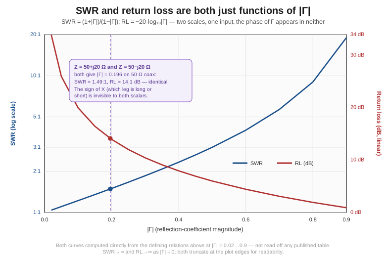
The discard, made concrete. Because SWR and RL depend only on |Γ|, any two loads that share a magnitude of Γ but differ in its phase are indistinguishable to both quantities — and, since a diode-based SWR bridge only ever recovers |Γ| in the first place, indistinguishable to that instrument at the hardware level, not merely on its display. Take two impedances symmetric about the resistive part of 50 Ω coax, Z₁ = 50 + j20 Ω and Z₂ = 50 − j20 Ω:
Γ₁ = (50+j20−50)/(50+j20+50) = j20/(100+j20) = 0.0385 + j0.1923, |Γ₁| = 0.1961
Γ₂ = (50−j20−50)/(50−j20+50) = −j20/(100−j20) = 0.0385 − j0.1923, |Γ₂| = 0.1961
The two reflection coefficients are complex conjugates of each other — same magnitude, opposite phase — exactly what you would expect from a pair of impedances that differ only in the sign of their reactance. Both give SWR = 1.49:1 and RL = 14.1 dB, computed directly from |Γ| = 0.1961 by the formulas above. A scalar SWR meter reading either load reports the identical number, “1.49:1,” and has no way to tell you which one you are looking at. But the two loads are not remotely interchangeable in practice: Z₁ is an antenna trimmed slightly long (inductive reactance above resonance is the signature of extra length on a wire element), and Z₂ is the same antenna trimmed slightly short (capacitive reactance below resonance) — the trim direction that fixes one is exactly backwards for the other. This is the precise, worked-through version of the informal claim that a scalar SWR meter “tells you 1.5:1 but not whether the reactance is inductive or capacitive”; the arithmetic above is what actually stands behind it, computed directly rather than merely asserted.
This is the entire reason the trim-and-sweep loop in both the single-band dipole dive’s DIY build volume and the fixed-vertical-monopole dive’s equivalent volume reads impedance and reactance sign off the analyzer rather than trimming by SWR alone — a builder chasing SWR alone can watch the number improve, worsen, or hold steady while cutting in the wrong direction, because SWR structurally cannot tell “too long” from “too short.” Reading R + jX (or the Smith-chart position derived from it in Section 5) removes the ambiguity, because the sign of X is preserved all the way from the reflected-wave phase measurement through to the display. A NanoVNA can, of course, still display SWR and return loss — they remain useful summary numbers for a quick “how bad is the mismatch” read, and both Section 4 and the workflow volumes lean on them for exactly that. The point of this section is narrower and more important: know which number you are reading, and know precisely what it cannot tell you.
1.4 The 2-port S-parameter set and the reference plane
Section 2 defined Γ for a single port — one line, one load, one reflected wave. A two-port device under test (a filter, a BALUN, a length of coax, an amplifier) has two ports, each capable of both receiving an incident wave and launching a reflected or transmitted one, and Section 2’s reflection coefficient generalizes into a 2×2 matrix of ratios called the S-parameters.
Definitions. Label the incident-wave sample at port 1 as a₁, the incident-wave sample at port 2 as a₂, and the corresponding outgoing-wave samples as b₁ and b₂. In general each outgoing wave is a linear combination of both incident waves,
b₁ = S₁₁a₁ + S₁₂a₂, b₂ = S₂₁a₁ + S₂₂a₂,
and the four S-parameters are recovered by measuring each ratio with the other port’s incident wave forced to zero — in practice, by terminating the other port in exactly Z₀, so nothing reflects off it back into the network:
S₁₁ = b₁/a₁ |a₂=0, S₂₁ = b₂/a₁ |a₂=0, S₁₂ = b₁/a₂ |a₁=0, S₂₂ = b₂/a₂ |a₁=0.
Physically: S₁₁ is the reflection coefficient looking into port 1 with port 2 perfectly terminated — an antenna’s S11 sweep, in the everyday sense, is exactly the Γ of Section 2, measured with the “port 2” side of the world (free space, in the antenna’s case) absorbing whatever gets through without reflecting anything back into the measurement. S₂₁ is forward transmission — the fraction (and phase) of the wave launched at port 1 that emerges from port 2 — and is the number a BALUN’s insertion loss or a filter’s passband response is read from. S₁₂ is the same thing run backwards, reverse transmission, and its difference from S₂₁ is what an amplifier’s reverse-isolation spec quantifies. S₂₂ mirrors S₁₁, the reflection coefficient looking into port 2 with port 1 terminated.
A precision worth being exact about: S₁₁ is not “Γ” — it is Γ under one specific condition. For amateur antenna work this distinction is usually invisible, because the “port 2” side of an antenna measurement is free space, which absorbs everything and reflects nothing back by construction — S₁₁ and Γ are the same number in that case. But in general, if port 2 is not terminated in Z₀ — if it sees some other load Γ_L — the actual reflection coefficient looking into port 1 is not S₁₁ alone; it picks up a contribution from however much of a₁ makes it through to port 2, bounces off Γ_L, and returns through the network a second time:
Γ_in = S₁₁ + (S₁₂S₂₁Γ_L)/(1 − S₂₂Γ_L).
This is the standard 2-port embedding relation, and it is worth carrying explicitly, because it is the reason “measure S11 of the antenna system” and “measure S11 of the antenna” are not automatically the same question once a lossy or mismatched feedline sits between the analyzer and the antenna — the feedline is itself a 2-port network with its own S-parameters, and the antenna’s true Γ_L gets folded through it by exactly this formula before the analyzer ever sees it. Vol 3’s field-measurement workflow, and the “measure at the rig end vs. the antenna end” question both sibling dives’ build volumes raise, is this formula wearing practical clothes.
What a 1-port-plus-transmission instrument can and cannot give you. A basic single-port reflectometer measures S₁₁ and nothing else — no transmission data at all, because it has no second sampled port. Adding a second receive channel that samples whatever emerges from port 2 (without adding a second source) gets you S₁₁ and S₂₁ in a single sweep — enough to characterize an antenna’s return loss and a filter or BALUN’s insertion loss, which covers the overwhelming majority of amateur antenna and matching-network work. What it does not get you, without further effort, is S₁₂ or S₂₂, because both require driving the network from port 2, and an architecture with only one source has no way to do that without physically reversing the device under test between the two ports and re-sweeping. Section 6 picks this exact limitation up as a direct consequence of the NanoVNA’s cost-reduced architecture; Vol 2 covers which hardware generations changed that trade-off.
The reference plane, generalized. Section 2’s single-port observation — that Γ’s phase rotates with electrical distance to the reference plane while its magnitude does not — applies to the full S-matrix as well, and it is the concept that makes calibration meaningful in the first place. An S-parameter is only a well-defined number once you have fixed where, physically, ports 1 and 2 are: the exact plane at which a₁, b₁, a₂, and b₂ are evaluated. Calibration — the open/short/load/through sequence covered in full in Vol 3 — is the procedure that pins that reference plane at the tip of the calibration standards, mathematically removing everything between the analyzer’s internal receivers and that physical point (connector parasitics, internal directivity error, cable delay) from the reported S-parameters. Move the reference plane afterward — add a barrel connector, a length of jumper cable, an adapter — and every S-parameter’s phase rotates accordingly, exactly as Section 2’s Γ(ℓ) = Γ(0)·e^(−2jβℓ) predicted for the single-port case; the magnitude of S₁₁ is unaffected by a lossless addition, while S₂₁’s phase (and, for a lossy addition, its magnitude too) shifts by the added path’s own insertion phase and loss. This is why “where exactly did you calibrate” is not a pedantic question — it is the difference between a measurement that means something and one that has an unknown length of coax silently folded into it.
A single worked number makes the effect concrete. Take a run of RG-58 (velocity factor ≈ 0.66, a widely quoted figure for that cable type) inserted between the calibration plane and the antenna, at 14.2 MHz. The free-space wavelength is λ = c/f ≈ 21.13 m; the guided wavelength on that cable is λ_g = 0.66 × 21.13 ≈ 13.95 m, giving β = 2π/λ_g ≈ 0.4505 rad/m. A single extra meter of that cable is a one-way electrical length of βℓ ≈ 0.4505 rad ≈ 25.8°, and by Γ(ℓ) = Γ(0)·e^(−2jβℓ) the round-trip phase rotation applied to the reported S11 is twice that, roughly 52° — with the magnitude of Γ untouched by a low-loss cable over that short a run. Those angles are arithmetic worked here from the defining phase-rotation formula and the quoted velocity factor, not a measured result or a figure read off a vendor chart. Fifty-two degrees is enough to walk a Smith-chart trace most of the way around a quadrant while the SWR reading at that frequency does not move at all, which is exactly why comparing a Smith-chart plot taken at the antenna’s feedpoint against one taken at the shack end of 30 m of coax is comparing two different reference planes, not two measurements of the same thing.
1.5 Impedance, Z, and the Smith chart as the same mapping
Section 2 derived Γ from Z; the same boundary condition inverts cleanly to recover Z from Γ, and the two directions are worth having side by side rather than memorized as separate facts.
Z from Γ. At the reference plane, V = V⁺(1+Γ) and I = (V⁺/Z₀)(1−Γ), so
Z = V/I = Z₀ · (1+Γ)/(1−Γ).
Γ from Z, rearranging, or equivalently normalizing z = Z/Z₀ and Γ = (z−1)/(z+1):
Γ = (Z−Z₀)/(Z+Z₀), or z = (1+Γ)/(1−Γ).
Both directions are exact, both are the same relationship written two ways, and — this is the point of the section — the Smith chart is nothing more than this mapping drawn as a picture. It is not a separate tool that happens to relate to Γ; it is a coordinate grid for the normalized-impedance plane (r = constant lines, x = constant lines), redrawn on top of the Γ-plane by the bilinear transformation z = (1+Γ)/(1−Γ). Writing Γ = u+jv and z = r+jx and carrying the mapping through algebraically produces two families of circles:
- constant-resistance circles:
(u − r/(1+r))² + v² = (1/(1+r))² - constant-reactance circles:
(u−1)² + (v−1/x)² = (1/x)²
Every “circle” on a Smith chart is one of these two families, evaluated at a specific r or x and clipped to the region |Γ| ≤ 1 (a passive impedance has r ≥ 0 and always maps inside or onto the unit circle — this is why the chart’s outer boundary is the unit circle, and why an active or negative-resistance device correctly plots outside it). The r = 0 circle is a special, degenerate case worth noticing on sight: substituting r = 0 gives center (0,0) and radius 1 — the entire outer boundary itself, which makes sense, because r = 0 means a purely reactive impedance, and any purely reactive load reflects 100% of incident power by definition (|Γ| = 1 for any Z = jX, a one-line check against the defining formula).
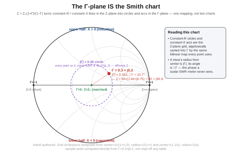
Figure 1 draws this grid directly — several constant-r circles, several constant-x arcs above and below the real axis, computed from the two formulas above rather than traced from a published chart — with one worked sample point, Γ = 0.3 + j0.2, carried through to Z = 50×(1.64+j0.75) ≈ 82 + j38 Ω on a 50 Ω system, so the mapping arithmetic can be checked rather than taken on faith. A dashed constant-|Γ| circle is also drawn through that region, tying this figure back to Section 3 directly: every point on that dashed circle shares the same SWR and the same return loss, and differs only in the reactance a scalar meter cannot see.
Reading the two halves. Because a positive-reactance load rotates Γ into the upper half-plane and a negative-reactance load into the lower half-plane (Section 2), the Smith chart’s upper half is universally the inductive region and its lower half the capacitive region — this is not a drafting convention, it falls directly out of the sign of Im(Γ) in the mapping. The center of the chart, Γ = 0, is the one point where Z = Z₀ exactly — a perfectly matched load, by definition, since there is nothing to reflect. The right-hand end of the real axis, Γ = +1, is the open circuit (Z → ∞); the left-hand end, Γ = −1, is the short circuit (Z = 0). Every other point on the real axis is a purely resistive impedance — above Z₀ to the right of center, below Z₀ to the left — and every point off the real axis carries a reactance whose sign you read from which half-plane it sits in and whose magnitude you read from which constant-x arc it lies on.
Why this matters more than it looks like it should. A builder who has internalized Section 3’s lesson — that SWR and return loss cannot distinguish inductive-and-long from capacitive-and-short — gets the distinction back for free the moment the same measurement is plotted on this chart instead of read as a scalar, because the chart is simply Γ’s phase and magnitude, undiscarded, drawn as a position rather than reported as two separate numbers. A trace sitting above the real axis is inductive; the antenna is too long, and the fix is to shorten it. A trace below the real axis is capacitive; the antenna is too short. This is exactly the physical content a scalar SWR reading throws away and a Γ-plane plot preserves — the chart is not a feature bolted onto S-parameter measurement, it is a direct visualization of the very quantity Section 2 defined as the instrument’s primitive output.
The admittance chart is the same mapping again, rotated. Normalized admittance is simply y = 1/z, and substituting z = (1+Γ)/(1−Γ) gives y = (1−Γ)/(1+Γ) — the identical bilinear form with the sign of Γ flipped. Geometrically, that sign flip is a 180° rotation of the entire chart about its center: the same grid of circles and arcs, the same unit-circle boundary, the same Γ = 0 matched point, but with the short-circuit and open-circuit ends swapped. A combined Z-Y chart (constant-r/constant-x circles overlaid with constant-conductance/constant-susceptance circles on the same disk) is nothing more than both rotations of one mapping drawn on the same page at once — which is why a shunt-element matching move (adding a capacitor or inductor across the line) reads as motion along a constant-conductance arc while a series-element move reads as motion along a constant-resistance circle: both are the same Γ-plane, viewed through z for one move and y for the other.
What this volume does not cover. Everything above is the mathematics the Smith chart encodes — the mapping, the two circle families, the half-plane convention, the special points. It is deliberately silent on the procedure of using a Smith-chart display on an actual NanoVNA screen: switching display modes, reading markers, or tracing a matching-network move along a constant-r circle and then a constant-conductance arc to walk an impedance to the center. That hands-on workflow, plus the on-device matching-network procedure both the fixed-vertical and dipole build volumes lean on, is Vol 4’s job in full.
1.6 What the NanoVNA actually is — bridge, mixer, synthesizer
Everything in Sections 2 through 5 is true of any vector network analyser, from a $50 NanoVNA to a $50,000 laboratory instrument. What differs between them is how the incident and reflected wave samples — a and b, Section 2’s V⁺ and V⁻ — actually get produced and turned into numbers, and a NanoVNA’s specific answer to that question is inseparable from its price. This section stays at the level of architecture, not model-by-model specification; the hardware family, generation by generation, is Vol 2’s job, and the concrete dynamic-range and drift numbers that architecture implies are Vol 5’s.
The front end: a resistive bridge, not a directional coupler. A conventional laboratory VNA separates the incident and reflected waves with a directional coupler — a piece of transmission-line hardware whose coupled port samples a wave travelling in one direction while remaining largely insensitive to a wave travelling the other way. A coupler’s directivity (how well it rejects the wave it is not supposed to sample) depends on physical length relative to a wavelength, and building one with good directivity down at 50 kHz — the low end of a typical NanoVNA sweep — would need coupled-line sections or transformers far too large for a handheld instrument. The standard low-cost answer, and the one consistent with everything documented about the openly-published NanoVNA hardware, is a resistive bridge reflectometer instead: a Wheatstone-bridge-like network of resistors that separates forward and reflected samples across a DC-to-GHz range no coupler can cover at the low end, at the cost of directivity that is modest by laboratory standards. That cost is not fatal — it shows up as a residual, repeatable directivity error, and the entire point of the open/short/load calibration sequence in Vol 3 is to characterize and cancel exactly that error mathematically, rather than eliminate it in hardware. This is a structural characterization of why a bridge is the sensible choice at this price point and frequency range, not a claim read off a specific schematic in this pass — Vol 2 is where per-model hardware detail gets verified against primary documentation.
The underlying principle is the same one behind any classic Wheatstone bridge: four impedance arms arranged so that, with a reference resistor in one arm exactly equal to Z₀, a perfectly matched load in the unknown arm drives the bridge’s sense terminals to a null — no signal at all reaches the “reflected” output, because the bridge is balanced. Any mismatch in the load unbalances the bridge by an amount proportional to Γ, and the sense terminals recover a non-zero signal whose amplitude and phase (relative to the stimulus) are Γ, extracted directly by the bridge topology rather than by timing a reflected pulse or separating counter-propagating waves on a length of line the way a coupler does. That is what makes a bridge frequency-independent down to arbitrarily low frequencies in a way a coupler structurally cannot be — a bridge’s balance condition depends only on the ratio of its resistor arms, never on a physical length being a usable fraction of a wavelength.
The synthesizer and the mixer. The openly-published NanoVNA firmware repository (ttrftech/NanoVNA on GitHub) identifies the stimulus and local-oscillator source as a Si5351A synthesizer chip, and the project’s own reference material identifies the downconversion stage as an SA612A mixer — or, on more recent boards, the pin-compatible NE602A that replaced it after NXP discontinued the SA612A/SA602A family in November 2022 — a double-balanced Gilbert-cell mixer. The synthesizer generates the RF stimulus fed toward the bridge and, simultaneously, a local-oscillator signal offset from it by a small amount; each mixer downconverts one of the sampled travelling waves (the forward sample a, the reflected sample b) against that same LO, moving both down to a common low intermediate frequency. Because both mixers share one LO, the phase relationship between a and b survives the downconversion intact — this shared-LO coherence is the hardware mechanism behind the word “vector” in vector network analyser, and it is exactly what a diode-detector scalar bridge lacks, since a diode detector has no LO to be coherent with in the first place. The resulting low-IF signals are digitized — the firmware repository’s own file listing shows a TLV320AIC3204 audio-band codec doing that job, alongside an STM32-family microcontroller — and the MCU extracts magnitude and phase from the digitized IF via synchronous detection, computing S₁₁ = b₁/a₁ (and, on a design with a second sampled port, S₂₁ = b₂/a₁) directly from those recovered phasors.
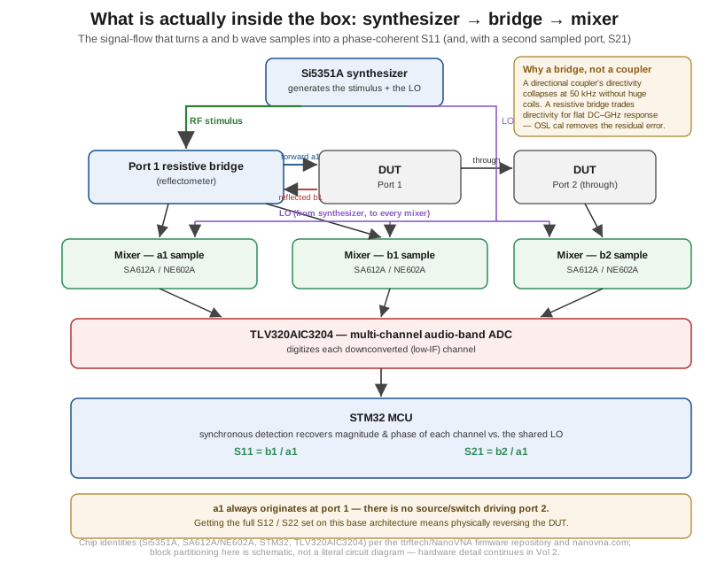
Figure 3 lays this signal path out as a block diagram, synthesizer through bridge to mixers, in the same order this paragraph describes it.
What the frequency range actually costs. The Si5351A’s own output range does not reach the multi-GHz territory some NanoVNA variants advertise; the extension above roughly 300 MHz is achieved by driving and sampling harmonics of the fundamental synthesizer output rather than a clean fundamental signal, at correspondingly reduced signal level and accuracy. The NanoVNA project’s own published material is explicit that a well-built unit reaches on the order of 40 dB of dynamic range at 900 MHz, that improved (H-series) hardware pushes that figure out to roughly 1.5 GHz, and that the noise floor and other measurement uncertainties become substantial above that point even though firmware may sweep the display considerably higher. That is a materially more conservative picture than a flat “50–80 dB across the board” figure would suggest, and the gap between the two is exactly the kind of unverified number this volume’s citation discipline exists to catch: hedge explicitly — this volume has not independently bench-verified any specific unit’s dynamic range, and Vol 5 is where the corrected, model-by-model picture belongs. The point to take here is structural rather than a specific dB figure: harmonic-mixing range extension and a single low-cost mixer chip both cost signal-to-noise headroom, and that cost grows with frequency, which is why every NanoVNA spec sheet in Vol 2 quotes better dynamic range at HF than at its upper frequency limit.
What a single source costs you. Section 4 already flagged the consequence directly: an architecture with one synthesizer driving one bridge at port 1, and a second receiver merely sampling whatever arrives at port 2, gives you S₁₁ and S₂₁ in a single sweep and nothing else — S₁₂ and S₂₂ are not obtainable without physically reversing the device under test and re-sweeping, because nothing in the signal path can drive a stimulus into port 2. A full four-parameter, no-DUT-reversal 2-port VNA needs a switched source (or two independent sources), so that either port can act as the stimulus origin in turn — hardware that costs more than a single bridge-mixer-synthesizer chain, which is exactly why it shows up on more expensive instruments and not on the base architecture described above. Every limit in this section — bridge directivity, harmonic-mixing range extension, single-source asymmetry — is a direct, traceable consequence of building a two-port S-parameter instrument for $50–300 rather than $5,000, and none of them prevents Sections 2 through 5’s physics from holding exactly as derived; they only bound how well, and over what range, this specific instrument can exploit that physics.
1.7 Where this volume hands off
This volume fixed the one idea the rest of the dive is built on: a vector network analyser measures a single complex quantity, the reflection coefficient Γ, at a defined reference plane — and SWR, return loss, complex impedance, and the Smith-chart trace are four different ways of looking at that one number, not four independent measurements. SWR and return loss are scalar functions of |Γ| alone and structurally cannot recover the sign of a load’s reactance, which two loads with conjugate impedances (Z = 50±j20 Ω, worked in Section 3) make concrete: identical SWR, identical return loss, opposite trim direction. The 2-port S-parameter set generalizes Γ to transmission as well as reflection, and the reference-plane concept — Γ’s phase rotating with electrical distance while its magnitude holds steady — is what makes calibration a meaningful, well-defined operation rather than an arbitrary ritual. Z = Z₀(1+Γ)/(1−Γ) and its inverse turn Γ into impedance in either direction, and the Smith chart is simply that bilinear mapping’s grid, not a separate chart. Finally, the NanoVNA’s own architecture — a resistive bridge standing in for a directional coupler, a Si5351A-class synthesizer and SA612A/NE602A-class mixer producing a phase-coherent downconversion, an STM32 extracting magnitude and phase from the result — is precisely what makes a $50–300 instrument capable of measuring Sections 2 through 5’s physics at all, and precisely what bounds how well it does so.
The dive continues from here into the instrument itself. Vol 2 surveys the NanoVNA hardware family in depth — the V2/V2.2 lineage, SAA-2N, Hugen H4, LiteVNA-64, and NanoVNA-F variants, what changed generation to generation, and how to choose among them. Vol 3 is the calibration discipline and the day-to-day measurement workflow: the open/short/load/through sequence that pins the reference plane, the S11 and S21 sweep procedures, and time-domain reflectometry for locating a feedline fault. Vol 4 puts Section 5’s mathematics to work as an on-device and host-software workflow — reading the trace, using NanoVNA-Saver, and the visual matching-network procedure both the fixed-vertical and dipole build volumes reference. Vol 5 closes the dive with the limits Section 6 set up — verified dynamic-range and calibration-drift figures in place of this volume’s structural argument for why they exist — followed by the buying guide and the common gotchas and myths a NanoVNA user runs into on the bench.
1.8 Resources
- Pozar, Microwave Engineering (4th ed.), Ch. 4 — S-parameters and 2-port network theory, the standard reference for the embedding relation and the Γ↔Z derivation this volume works through from first principles.
- P. H. Smith, “Transmission-Line Calculator,” Electronics, January 1939, with an expanded follow-up in 1944 — the original publication behind the graphical construction Section 5 re-derives analytically.
ttrftech/NanoVNAfirmware repository (GitHub) — the openly-published hardware bill of materials Section 6 draws from (Si5351A synthesizer, STM32-family MCU, TLV320AIC3204 codec).- nanovna.com (NanoVNA project reference material) — the mixer chip identity (SA612A/NE602A) and the frequency-range / dynamic-range figures cited in Section 6.
- ARRL Antenna Book (25th+ ed.) — the Smith chart and SWR/return-loss chapter, for the amateur-radio framing of the same mathematics developed here.
Comments (0)